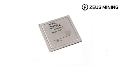
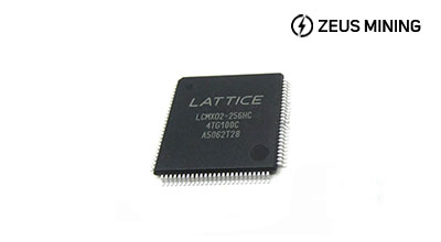
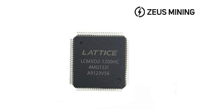
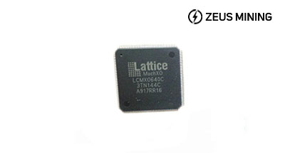
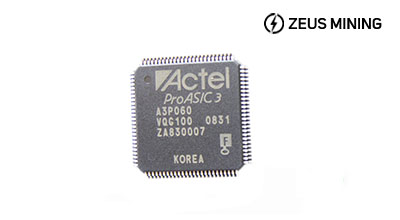
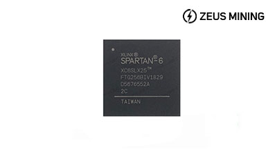
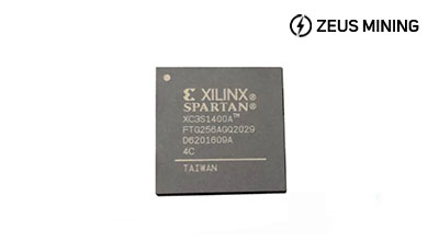
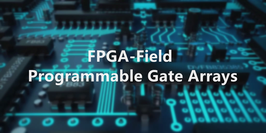
FPGA, Field Programmable Gate Array, is a product of further development based on PAL, GAL, EPLD, and other programmable devices. It emerged as a semi-custom circuit in the field of application-specific integrated circuits (ASIC), which solves the deficiencies of custom circuits and overcomes the shortcomings of the limited number of gate circuits of the original programmable devices. FPGA adopts a new concept of LCA (Logic Cell Array), which includes three parts: Configurable Logic Block (CLB), IOB (Input Output Block), and Interconnect. It can support one piece of PROM to program multiple pieces of FPGA; the serial mode can use the serial PROM to program the FPGA; the peripheral mode can use the FPGA as the peripheral of the microprocessor, and the microprocessor can program it. The new field programmable gate array (FPGA) has many logic gates and RAM block resources, which can realize complex digital calculations. Because FPGA designs use high-speed I/O rates and bidirectional data buses, it has become a challenge to verify the correct timing of valid data in the setup time and hold time.
Dear Customers,
Hello, May 1-5, 2026 (GMT+8) is China's May Day, and international logistics will be suspended. Our company will suspend shipments on the afternoon of May 1, 2026, and resume warehouse shipments on May 6 (GMT+8). We are deeply sorry for the inconvenience caused to you. Thank you for your trust and support.
Best wishes,
ZEUS MINING CO., LTD.