


Antminer S19 XP Hash Board Repair Guide
I. Maintenance Platform/Tool/Equipment Preparation Requirements
1. Platform requirements:
Anti-static repair workbench (the workbench needs to be grounded), the repairman must wear anti-static wrist straps.
2. Equipment requirements:
(1) Constant temperature soldering iron (350℃-380℃/662F°-716F°), pointed iron head is used for soldering small chips such as chip resistors and capacitors.
(2) Heat gun and heating platform (350℃-400℃).
(3) BGA repair workbench is suitable for chip / BGA disassembly and soldering.
(4) Multimeter (Fluke 17B+ is recommended) is equipped with a welded steel needle and a heat-shrinkable sleeve for easy measurement.
(5) Oscilloscope (UTD2102CEX+ oscilloscope is recommended).
(6) Network cable (Requirement: connected to the Internet, stable network).
3. Test tool requirements:
(1) Use the APW12 power supply (APW1212V-15V and power adapter cable) to build a test platform: Use thick copper wires for the positive and negative poles of the power supply, and then connect the PSU and the hash board. It is recommended to use 6AWG copper wires with a length of less than 60cm for the hash board powering.
(2) Use the test fixture of the V2.1010 control board (its model is ZJ0001000001), the positive and negative poles of the power supply of the test fixture need to be installed with a discharge resistor, and it is recommended to use a cement resistor of 25 ohms and above 100W.
4. Repair auxiliary materials:
Solder paste M705, flux, board washing water, absolute alcohol, thermal conductive gel, ball planting steel mesh, solder absorbing wire, solder ball (ball diameter recommended 0.4mm)
(1) Circuit board cleaning solution is used to clean up the flux residue after maintenance
(2) Thermally conductive gel (specification: FujipolySPG-30B) is applied on the surface of the chip after maintenance.
(3) When replacing the chip, it is necessary to plant tin on the pins of the chip first, and then solder it to the hash board. Apply heat-conducting gel evenly on the surface of the chip and then install the large heat sink.
5. Repair auxiliary tools:
(1) Scanning gun: recommended ZD2200 Wired Scanner
(2) Adapter board RS232/TTL adapter board 3.3V
(3) Self-made short-circuit probes are soldered with needle wires, need to add heat-shrinkable sleeves to prevent short-circuiting between the probes and the small heat sink.
6. Common maintenance spare material requirements: 0402 resistors (0R, 51R, 10K, 4.7K), 0402 capacitors (0.1uF, 1uF).
II. Job Requirements
1. Maintenance personnel must have certain electronic knowledge, more than one year of maintenance experience, and be proficient in BGA/QFN/LGA packaging and soldering technology.
2. After maintenance, the hash board must be tested twice or more and the results are 0K, in order to pass!
3. Pay attention to the soldering technique when replacing the chip. After replacing any accessories, the PCB board will not be deformed. Check the replaced parts and surroundings for missing pieces, open circuits and short circuits.
4. For the test of chip maintenance and replacement, it is necessary to detect the chip first, and then do a functional test after passing. The functional test must ensure that the small heat sink is soldered well and the large heat sink is installed in place (each thermal conductive adhesive must be applied evenly before installing the large heat sink). And the cooling fan is at full speed. To use the chassis for heat dissipation, two hash boards must be placed at the same time to form an air duct. The single-sided test of production must also ensure the formation of an air duct (important).
5. When powering on the hash board, you must first connect the negative copper wire of the power supply, then the positive copper wire of the PSU, and finally insert the signal cable. When disassembling, the order of installation must be reversed, first remove the signal cable, then remove the positive copper wire of the power supply, and finally remove the negative copper wire of the power supply. If you do not follow this order, it is very easy to cause damage to U1 and U2 (not all chips can be found); Before testing the pattern, the repaired hash board must be cooled down before testing, otherwise it will result in testing PNG.
6. Determine the maintenance station object and the corresponding test software parameters and test fixtures.
7. Check whether the tools and test jig can work normally.
8. The fan plays a cooling role when measuring the signal, and it is necessary to keep 4 fans running at full speed.
9. When replacing a new chip, clean the pins and apply solder paste to ensure that the chip is coated with tin before soldering.
III. Production and precautions of test fixture
1. Fixture model: ZJ0001000001 test fixture.
2. For the first time use the 19 series test fixture SD card flash program to update the FPGA control board of the tester, copy it to the SD card after decompression, and insert the SD card into the fixture card slot: Power on for about 1 minute, and wait for the red and green indicators on the control board to flash 3 times in succession, then the update is complete (if it is not updated, it may cause a fixed chip to be reported as defective during the test).


3. Make the SD card according to the requirements. When the hash board is only installed with a single-sided heat sink and detect the chip, directly decompress the compressed package to make the SD card;
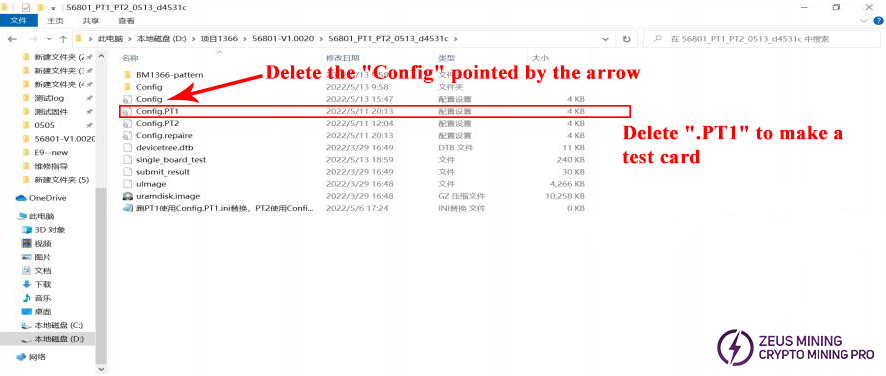
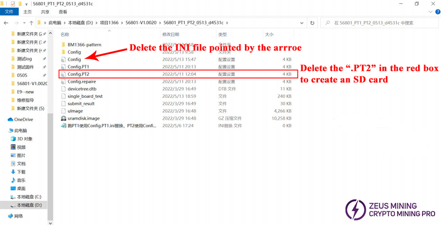
4. Make the SD card according to the requirements, double-sided heat sink, 8 times Parrer test, you need to make the SD card as shown in the figure below:
IV. Principle and Structure of hash board
1. Working structure of S19 XP hash board:
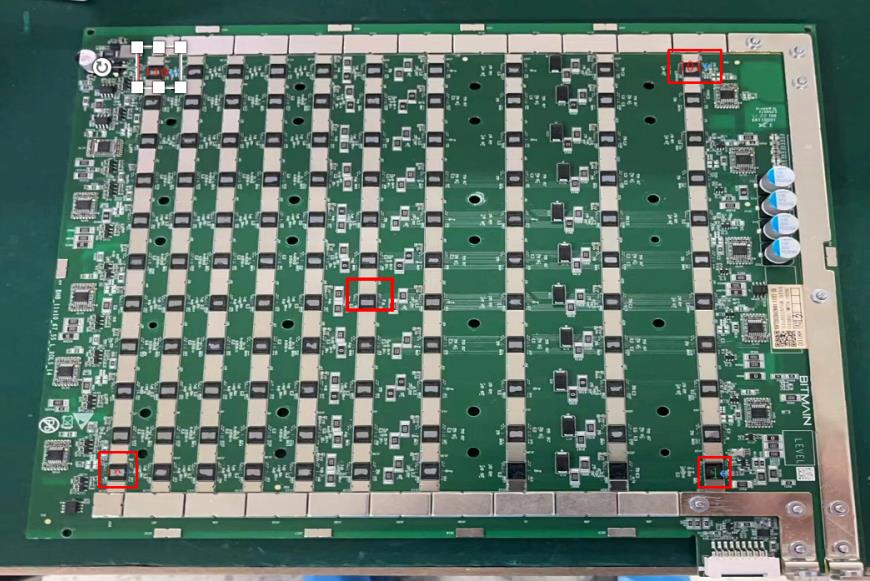
The S19 XP hash board is composed of 110 BM1366 chips, which are divided into 11 domains, and each domain is composed of 10 ASIC chips.

3. S19 XP chip signal direction:
1) CLK (OUT) signal flow direction, generated by Y1 25M crystal oscillator, transmitted from chip 01 to chip 110; (0.6-0.7V)
2) The TX (CI, CO) signal flows in from pin 7 (3.3V) of the IO interface, and then transmits from chip 01 to chip 110 after the level conversion IC U10; the voltage is OV when the I0 cable is not inserted, and the operation voltage is 1.2V;
3) The RX (RI, RX) signal flows from chip 110 to chip 01, returns to the 8th pin of the signal cable terminal through U2, and finally returns to the control board; the voltage is 0.3V when the IO cable is not plugged in, and the voltage during operation is 1.2V:
4) BO (BI, BO) signal flow direction, from chip 01 to chip 110;
5) The flow direction of the RST signal enters from pin 3 of the IO interface, and then transmits from chip 01 to chip 110; its voltage is 0V without an IO line or in standby, and the voltage during operation is 1.2V;
4. Machine structure:
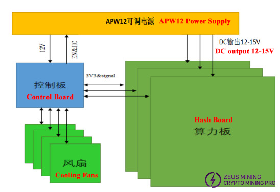
The whole miner is mainly composed of 3 hash boards, 1 control board, 1 APW12 power supply, and 4 cooling fans.
Ⅴ. Common faults and troubleshooting steps of Antminer S19 XP hash board
1. Phenomenon: the single board test detects that the chip is 0 (PT1/PT2 mode)
Step 1: check the power supply's output;
Step 2: check the voltage output of the voltage domain;
The voltage of each voltage domain is about 1.35V. If there is a 14V powering, there is generally a domain voltage, and the output of the power terminal of the hash board is measured first; if there is a 14V powering but no domain voltage, continue to check down.
Step 3: check the output of the boost circuit;
Test the EC5 in the figure below, and the voltage of 18V_19V can be measured.
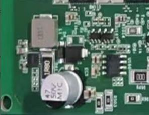

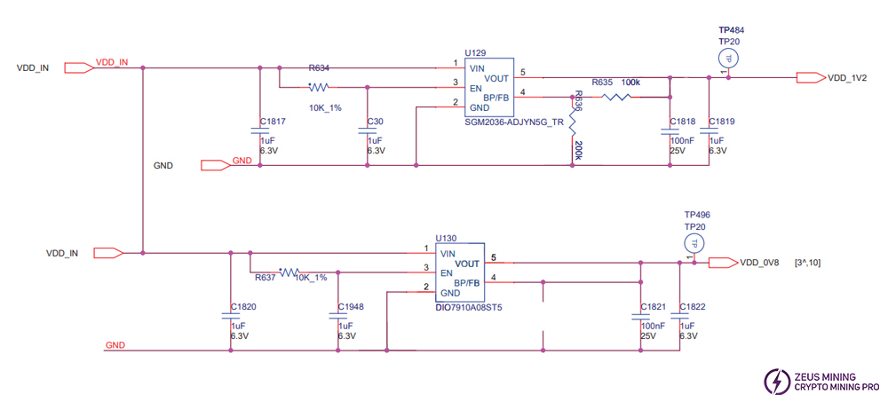
Step 4: check each group of LDO (linear regulator) 1.2V or PLL (phase locked loop) 0.8V output.
Step 5: check the signal output of the chip (CLK/CI/RI/BO/RST)
Refer to the voltage value range described by the signal trend. If the measured voltage value is too large, it can be compared with the measured values of adjacent groups for judgment.
PS: If the hash board is not powered or powered off according to the test sequence, causing U2 and U10 to burn out, it will report 0 when testing the chip;
Step 6: When EEPRXM NG is displayed on the LCD screen of the test fixture, check whether U6 is soldered normally;
Step 7: The temperature sensor is located on the side of chips, and the resistor is located on the front of the PCB. Check the soldering of the temperature sensor IC, whether the nearby resistors are damaged, and whether the 3.3V powering of the temperature sensor is normal; Check the chip connected to the temperature sensor. The material deformation of the large heat sink will cause poor heat dissipation of the chip and affect the temperature difference.
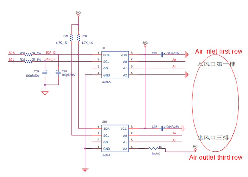
2. Phenomenon: The detection chip of the single board is incomplete (PT1/PT2 mode)
(1) When ASICNG=(0) is displayed: first measure the total voltage of the domain and the 19V boost circuit is normal, and then use a short-circuit probe to short the RX test point and 1V2 test point between the No.1 and No.2 chip. Then run the check chip program and see the serial port log. If you still find 0 chip at this time, it will be one of the following situations:
① Use a multimeter to measure whether the voltages of the 1V and 0V8 test points are 1.2V and 0.8V. If not, it can be judged that the 1.2V and 0.8V LDO circuits in this domain are abnormal, or that the two ASIC chips in this domain are not soldered well, or that the 0.8V and 1.2V patch filter capacitors are short-circuited, or the IC of the LDO circuit in this domain has weak soldering/false soldering/material damage;
② Detect whether the circuits of U1 and U2 are abnormal, such as resistor in poor soldering, etc.;
③ Use a multimeter to measure the resistor of R8 or R9 to see if it is within 10 ohms, and the reading will not jump randomly. If not, replace both resistors;
④ Detect whether the pins of the first chip are not soldered properly (there are tins on the pins from the side during the repair process, but after removing the chip, it is found that the pins are not stained with tin);
⑤ Check whether the capacitor from R1104 to the booster circuit is disconnected.
(2) If 1 chip can be found in step (1), it means that the first chip and the previous circuit are both good. Use a similar method to check the subsequent chips. For example, short-circuit the 1V2 test point and the RX test point between the 38th and 39th chips. If the log can find 38 chips, there is no problem with the first 38 chips; if you still find 0 chip, check whether the 1V2 is normal, if it is normal, there is a problem with the chip after No. 38. Continue to use the binary method to check until the problematic chip is found. Assuming that there is a problem with the Nth chip, when the 1V2 and RX between the N-1th chip and the Nth chip are short-circuited, the N-1 chip can be found; However, when the 1V2 and RX between the N and N+1 chips are short-circuited, the full chip cannot be found.
(3) When ASICNG is displayed: (Fixedly report a certain bit chip), there are two situations as follows:
① The first case: (usually the value of the reported chip will not change every test), this case is likely to be caused by abnormal soldering of the front and rear CLK, CI, BO of the X-th chip, so focus on these 6 resistors. The small probability is that among the three chips X-1, X, and X+1, the following pins of the chips are abnormally soldered;
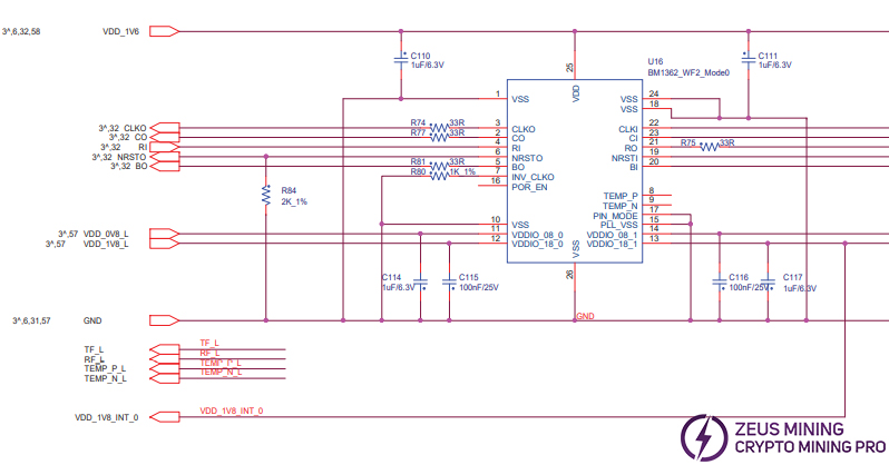
② The second case: Micro-short circuit between signals (0-hundreds of ohms), caused by the small resistor value of the chip pins, first use a heat gun to solder and see if it is OK;
3. Phenomenon: During PT1 test, when the chip is an integer, such as 10/20/30/40/50/60/70/80/90/100.
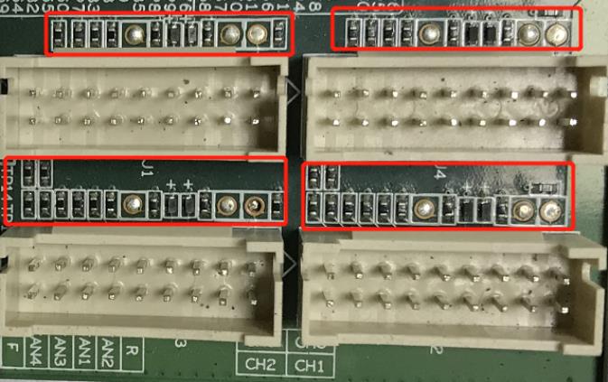
(1) When the integer is reported, it is necessary to check whether the Level shift small board is welded well, and to check whether the components on the small board have false soldering. If there is false welding, it needs to be re-soldered. If there is damage, it needs to be measured whether the resistance value is normal. Replace the corresponding components abnormally, and check the small board soldered on the PCB; the small board is shown in the figure below.
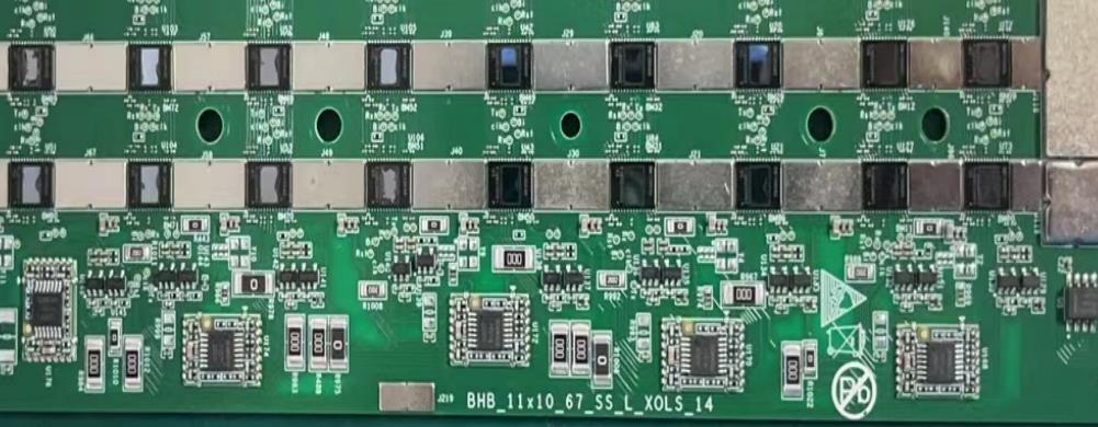
(2) When the chip still reports an integer number after confirming the small board, first check whether the RX signal is normal, and also measure whether the chip points 1.2V and 0.8V are normal, if not, confirm whether it is a connection problem, and re-solder if the soldering problem is , if the chip is bad, it needs to be confirmed by swapping.
4. Phenomenon: The single board test shows PatternNG, that is, the reply nonce data is incomplete (PT2 mode)
PatternNG is caused by the large difference between the characteristics of the chip and other chips. If the chip is damaged, it is usually only necessary to replace the chip.
According to the log information, the replacement rules are:
(1) Check the printing quality of thermal gel;
(2) If the appearance of the chip is not damaged, just replace the chip with the lowest response rate in each domain;
(3) Swap the one with a higher reply and the one with a lower reply. After the swap, test the hash board again to check whether the reply of the ASIC chip is normal. If it is abnormal, measure whether the voltage in this domain is lower than the normal value. Measure whether the resistance value of the chip pad pin is the same as normal, if not, check whether the resistance value of the small resistor next to it is too high, if it is too high, just replace it;
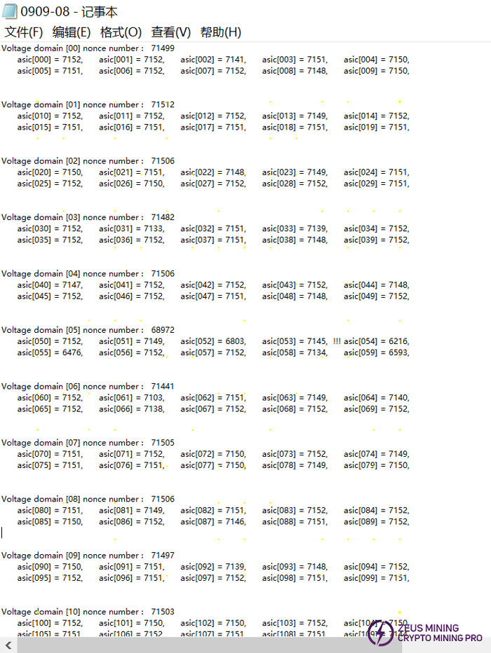
As shown in the figure below, it is one of the log tests. From the log, it can be seen that the response rate of the four chips of asic[70] [71] [78] [79] is low. 78 and 79 are in the same domain, and 70 and 71 are also in the same domain, so swap 78, 79 and other normal domains (such as the first domain). If it is still PNG, replace the chip.
PS: Special attention should be paid to the numbering of domain and asic starting from 0.
5. Phenomenon: Check the chip test OK, PT2 function test serial port does not stop (long-distance running)
Repair method: During the PT2 test, check the serial port print log, and then use the short-circuit probe to short-circuit the RX and 1.2V test points when the serial port starts to long-distance run, and start short-circuiting from the first chip. If the serial port stops long-distance running after the short-circuit, it means the first chip is OK. According to this method, find the chip that still fails after a long-distance running after a chip short circuit. Generally, it is caused by a damaged chip, and you can replace it;
6. Phenomenon: PT1 checks the chip test OK, PT2 function test fixedly reports a certain chip NG
Repair method: check the appearance, measure the chip capacitor or resistor in front, it is usually caused by poor soldering of the chip or a damaged chip capacitor or resistor or abnormal resistance value;
7. Phenomenon: B-AXPCS (Insufficient response of X chips)
Repair method 1: Measure whether the domain voltage of the reset low chip domain is lower than the normal domain, if it is lower, measure whether the pin resistance of the reset low chip is higher than that of the normal chip. If yes, you need to replace the chip; if not, measure the resistance value of the resistor next to it, and replace it if the resistance value is too large;
Repair method 2: Swap the chip with a high response and the chip with a low response;
VI. Common faults and troubleshooting steps of the control board
1. The whole miner does not run
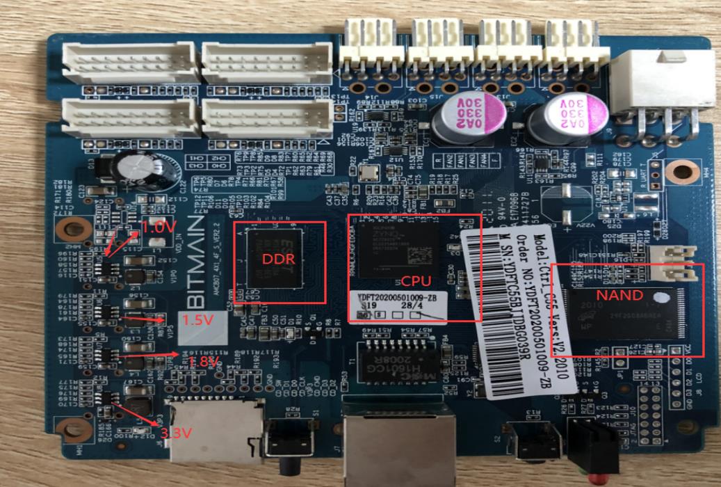
(1) Check whether the voltage of several voltage output points is normal. If the 3.3V is short-circuited, you can disconnect U8 first. If the short-circuit is still present, you can unplug the CPU and measure again. Other voltage abnormalities generally replace the corresponding voltage converter IC.
(2) The voltage is normal, please check the soldering status of DDR/CPU.
(3) Try to update the flash program with SD card.
If the miner whose control board is flashed needs to start normally, the following two steps are required:
① After the card is swiped successfully, the green LED indicator is always on, and the power is turned off and restarted at this time;
② Wait for 30s after power on again (the time course of turning on OTP);
③ OTP (0neTimeProgramable) is a memory type of MCU, which means one-time programmable. After the program is burned into the IC, it cannot be changed and cleared again.
Precautions:
(1) Sudden power failure or less than 30s in the process of opening OTP will cause the control board to fail to open the OTP function, and the control board will not start (not connected to the Internet). Need to replace U1 (control board main control IC FBGA), the replaced U1 cannot be used on Antminer 19 series miners;
(2) For control boards with OTP function enabled, U1 cannot be used on other series of models.
2. The whole miner cannot find the IP
(1) There is a high probability that the IP cannot be found due to abnormal operation, refer to point 1 for troubleshooting;
(2) Check the appearance and soldering conditions of the network port, network transformer T1, and CPU.
3. The whole miner cannot be upgraded
Check the appearance and soldering condition of the network port, network transformer T1, and CPU.
4. The whole miner fails to read the hash board or there are few chains
A. Check the cable connection status;
B. Check the parts of the control board corresponding to the chain;
C. Check the wave soldering quality of the pins and the resistors around the plug-in interface.
VII. Fault phenomenon of the whole miner
1. Preliminary test of the whole miner
(1) Fan abnormalities are displayed: Check whether the fan works normally, whether the connection with the control board is normal, and whether the control board is abnormal.
(2) Less chains: it means that one of the three hash boards is missing. In this case, most of the problems are caused by the connection between the hash board and the control board. Check whether there is an open circuit in the cable. If there is no problem with the connection, you can perform the PT2 test on the single board to check whether the test can pass. If it can be passed, most likely the control board is faulty. If the test fails, use the PT2 maintenance method to repair.
(3) Abnormal temperature: The maximum PCB temperature set by our monitoring system cannot exceed 90C/194T. If it exceeds 90C, the miner will alarm and cannot work normally. Generally, it is caused by the high ambient temperature. In addition, abnormal fan operation can also cause abnormal temperature.
(4) Unable to find all chips: (The miner can run, but the hashrate is 2/3 or 1/3 of the normal value) The number of chips is not enough, you can refer to PT2 for test and repair.
(5) After running for a period of time, there is no hashrate, and the connection to the mining pool is interrupted. Check the network.

(6) The single board test is OK, but the hashrate is low after being assembled into a complete miner for testing.
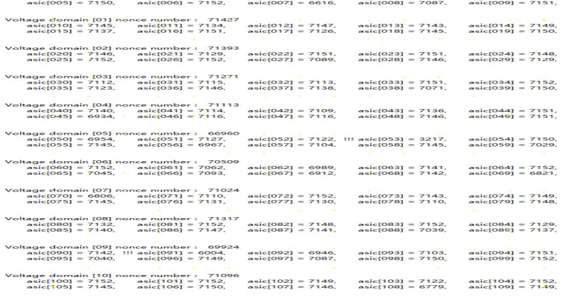
As shown in the figure below, the first hash board has no hash rate after running for about 3 minutes.
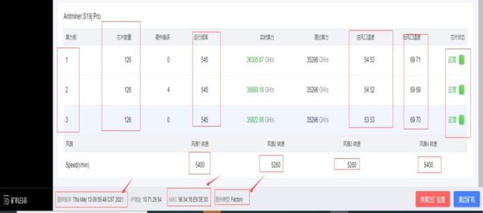
① The specific analysis method is as follows: First, conduct a single-board PT2 test to check whether the performance of the hash board is normal. If the test chip is not fully detected, the board needs to be repaired. If it is normal after the test, take out the hash board separately, use the test fixture to carry it into the Debug master program to mine, and adjust the fan speed to 95%.
a) Adjust the voltage and frequency to the working voltage and frequency of the whole miner, let the miner perform mining, and check whether there is a decrease in the hash rate.
b) If the miner still reduces the hash rate, then reduce the frequency to 200M, and keep other conditions unchanged. Let the miner perform mining to see if there is a decrease in hashrate and whether the hash board will display X.
c) If the hashboard still displays the X and reduces the hashrate, you can remove the heat sink of the hash board for mining. When the hashrate is reduce, measure whether the domain voltage is normal. In general, the domain voltage will be abnormal in the problematic domain. Then measure the RI signal to see where the RI signal is interrupted. If the RI signal disappears, it can basically be determined that the chip is short-circuited or damaged after being tinned.
② Another repair method: Log in to the IP through the "Putty" software to check whether the domain operating voltage of the hash board is normal, and whether the nonce return is normal, and you can repair according to the log information on the "Putty" software.
a) Open the software "Putty", enter the IP of the problematic miner, and click "Open".
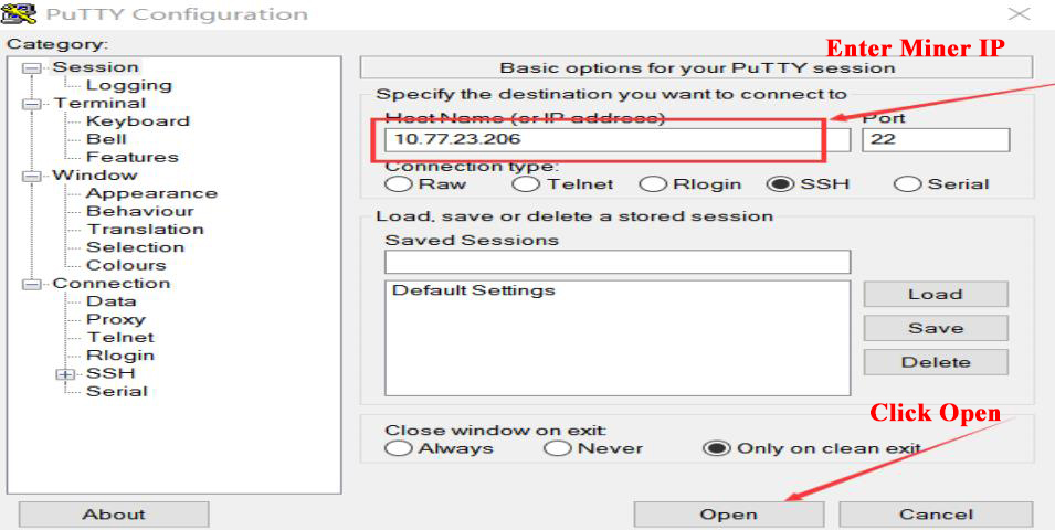
b) Enter the user name, password and the test command to see the NONCE return status and the status of the voltage domain. If there is abnormality in NONCE and domain voltage, it can be repaired according to the abnormal chip printed. There are two types of account passwords: one account is RXot, the password is admin; the other account is miner, the password is miner. This software can be used with Debug software at the same time.

Ⅷ. Others Precautions
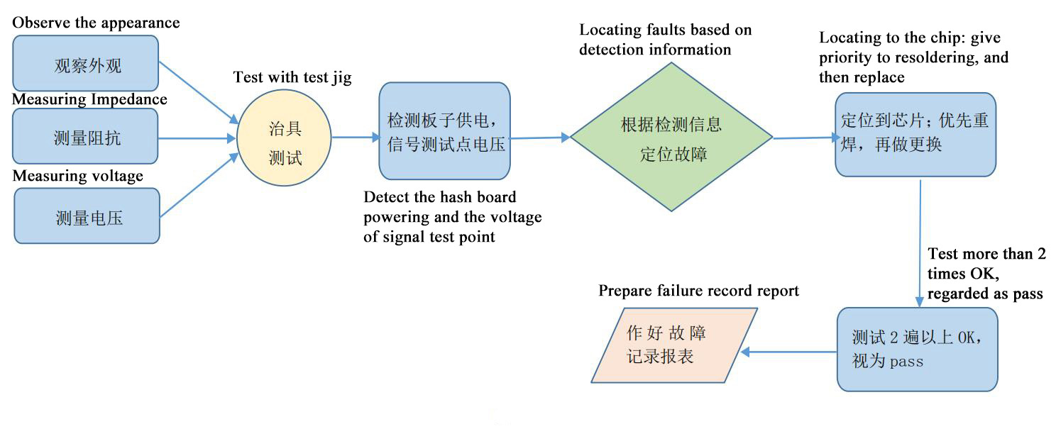
Maintenance flow chart:
1. Routine testing:
① First of all, visually inspect the hash board to see if there is any deformation or burning of the PCB. If there is any phenomenon, it must be dealt with first.
② Visually inspect whether there are obvious signs of burnt parts, parts impact offset or missing parts, etc.
③ After the visual inspection is OK, the impedance of each voltage domain can be detected to detect whether there is a short circuit or an open circuit. If found, it must be dealt with first.
④ Check whether the voltage of each domain is about 0.36V.
2. After the routine inspection is OK (short circuit detection of general routine inspection is necessary, so as not to burn the chip or other materials due to short circuit when the power is turned on), the chip can be tested with the test fixture, and the judgment and positioning can be carried out according to the test result of the test fixture;
3. According to the display results of the tester, start from the vicinity of the faulty chip, and check the chip test points (CO/NRST/RX/XIN/BI) and voltages such as VDD0V8 and VDD1V2.
4. According to the signal flow direction, in addition to the RX signal reverse transmission (No. 110 to No. 1 chip), the other several signals CLK CO BO RST are forward transmission (1-110), find the abnormal fault point through the powering sequence.
5. When the faulty chip is located, it is necessary to re-solder the chip. The method is to add flux (preferably no-clean flux) around the chip, and heat the solder joints of the chip pins to a dissolved state, so that the chip pins and pads are re-run-in and tin is collected to achieve the effect of re-tinning. If the same fault still exists after re-soldering, the chip can be replaced directly.
6. The repaired hash board needs to be tested with a test fixture, and it must pass more than two times to be judged as a good product. For the first time, after replacing the accessories, wait for the hash board to cool down, use the test fixture to test, and when is passed, put it on one side before cooling down. The second time, wait for the hash board to cool down completely before testing.
Dear Customers,
Hello, May 1-5, 2026 (GMT+8) is China's May Day, and international logistics will be suspended. Our company will suspend shipments on the afternoon of April 30, 2026, and resume warehouse shipments on May 6 (GMT+8). We are deeply sorry for the inconvenience caused to you. Thank you for your trust and support.
Best wishes,
ZEUS MINING CO., LTD.