


Antminer S19 XP Hydro Hash Board Repair Guide
Ⅰ. Maintenance platform/tool/equipment preparation requirements
1. Platform requirements:
Static repair workbench (the workbench needs to be grounded), anti-static bracelet and grounding.
2. Equipment requirements:
Constant temperature soldering iron (350℃ to 380℃), pointed soldering iron tip is used to solder small chips such as chip resistors and capacitors. Heat gun (350±10℃) and BGA rework station are used for chip/BGA disassembly and soldering. Multimeter add a welded steel needle and cover it with a heat shrink tube for easy measurement (Fluke is recommended). Oscilloscope, cable (requirements: connected to the Internet and stable network).
3. Requirements for repair test tools:
APW11 PSU (material number: C05010000110), the calibrated power supply APW111721d_17V-21.6V_V1.10 must be used for PT2 testing in production lines. DIY power adapter cable: Use thick copper wires for the positive and negative poles of the power supply to connect the power supply and the hash board. It is recommended to use 4AWG copper wires with a length of less than 60cm for power to the hash board. Use 19 series universal test fixture (Part No. ZJ0001000001 / ZJ0001000004)
PT1 test supports APW9 and APW9+ power supplies.
4. Requirements for repair auxiliary materials/tools:
Solder paste M705, flux, board washing water with anhydrous alcohol (board washing water is used to clean up the flux residue after repair). Thermal grease (used to apply on the chip surface after repair). Tin-planted steel mesh (6mm * 7mm chip size), desoldering wire. When replacing a new chip, need to tin the chip pins and then solder them to the hash board. Apply thermal conductive silicone grease evenly on the chip surface and then lock the water-cooling heat sink.
5. Common repair spare material requirements:
SMD resistor 33Ω 1% 1/20W 0201(0603), SMD resistor 10KΩ +/-1% 1/16W 0402, SMD resistor 0Ω 5% 1/16W 0402. SMD ceramic capacitor 1uF +/-10% 16V X5R 0402, SMD ceramic capacitor 1uF 6.3V 20% X5R 0201(0603), SMD ceramic capacitor 22uF +/-20% 6.3V X5R 0603.
Ⅱ. Repair requirements
1. Pay attention to the working method when replacing the chip. There will be no obvious deformation of the PCB board after replacing any accessories. Check whether there are open or short circuit problems in the replacement parts and surrounding parts.
2. Maintenance personnel must have certain electronic knowledge, more than one year of repair experience, and be proficient in BGA/QFN/LGA packaging welding technology.
3. After repair, the hash board must be tested more than twice and both are OK before it can pass!
4. Check whether the repair tools and test fixtures can work normally, and determine the repair station test software parameters, test fixture versions, etc.
5. When repairing or replacing a chip, you need to test the chip first and then do a functional test after passing it. The functional test must ensure that the water-cooling plate is assembled properly. When installing the water-cooling plate, the surface of the chip must be evenly coated with thermal conductive silicone grease. The cooling fan is at full speed, or a water-cooling radiator and water row are connected. When connecting a water row for heat dissipation, a water pump needs to be added to the water inlet to increase the water flow rate.
Note: Testing PT1 without a radiator on the single board will cause the chip to overheat and burn the board (must be careful).
6. When checking the chip measurement signal of PT1, be sure to lock the radiator to avoid burning the board. The PT2 test needs to be connected to the water row, and the water flow rate is 3-3.5L/min to test. The water temperature requirement is between 30 and 35°C. Testing will not be possible if the water temperature is below or above this temperature.
7. When connecting the radiator to measure signals and voltages, measurements can be made on the BOT surface. The bottom bracket has reserved openings for easy measurement of signal voltage points.
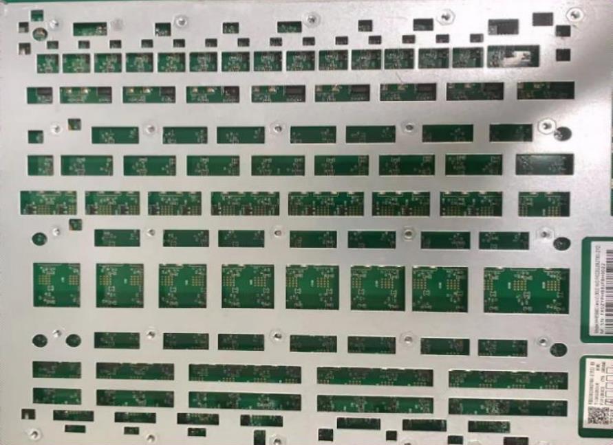
8. When replacing a new chip, the pins and solder paste must be printed to ensure that the chip is pre-tinned and then soldered to the PCBA for repair.
9. After the PCBA with the heat sink removed is repaired, the water-cooled radiator must be re-printed with thermal grease. Then perform post-installation testing (otherwise it will cause instability in the long run of the whole machine).
Ⅲ. Fixture production and precautions
The fixture should satisfy the heat dissipation of the hash board and facilitate signal measurement.
1.Material number: ZJ0001000001 test fixture.
2.When using the S19 XP Hyd. series test fixture for the first time, use the SD card flash program to update the FPGA on the fixture control board. After decompression, copy it to the SD card and insert the card into the fixture card slot. Power on for about 1 minute and wait for the indicator light on the control board to double flash three times before the update is completed (if it is not updated, a certain chip may be reported as defective during the test).

Figure 3-1
3. The test SD card will be made according to the requirements, and the PT1 detection chip and PT2 function test will be directly unzipped to make the SD card. After unzipping, delete the original Config file first, name the Config.ini-HHB42601-PT2 configuration file Config.ini, and then click "Yes". The final configuration file is "Config.ini". (The repaired board must be streamlined again from PT1 according to the production process. Maintenance personnel are not allowed to skip the test assembly without permission)
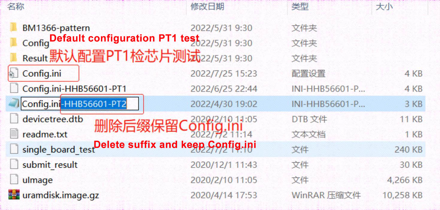
Figure 3-2
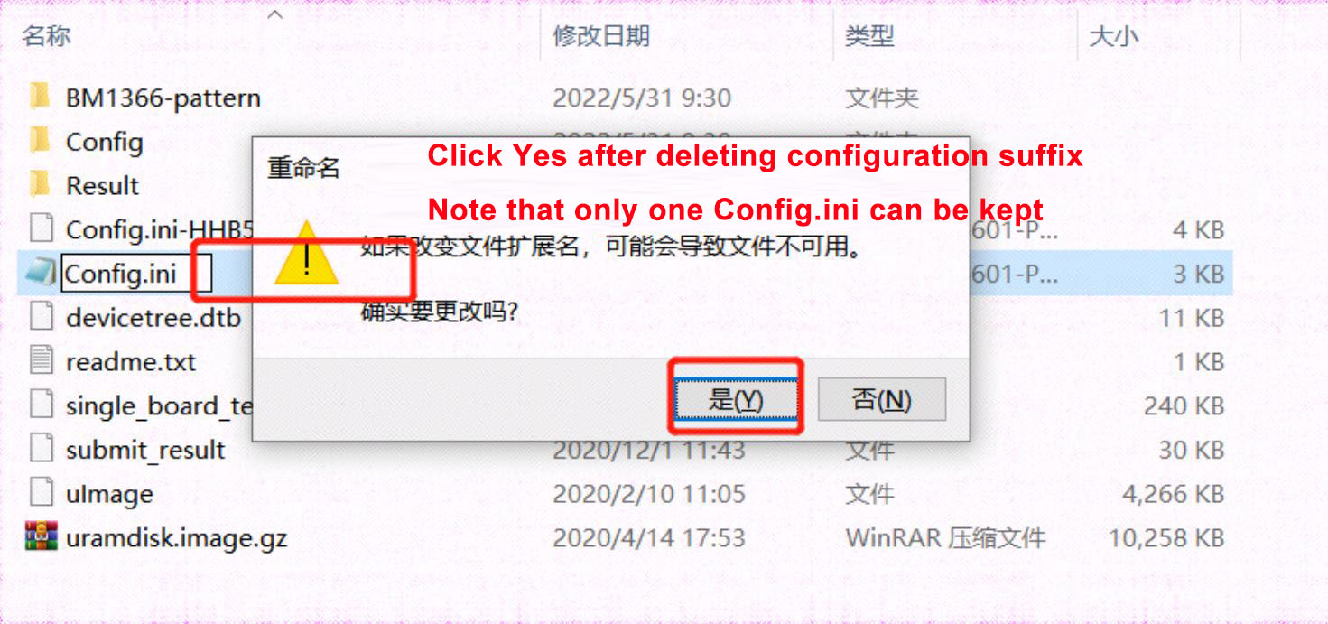
Figure 3-3
Ⅳ. Principle Overview
1.S19 XP Hyd. (HHB56601) hash board working structure:
The hash board consists of 204 BM1366 chips (PCB silk screen order BM1 to BM204), divided into 17 groups (domains), each domain consists of 12 ASIC chips. The operating domain voltage of the BM1366 chip used in the S19 XP Hyd hash board is around 1.14 to 1.25V. The chip VDDIO of domains 1 to 15 is powered by 1.2V&0.8V LDO. Each domain uses 4 LDOs for power supply (one LDO outputs 1.2V and 3 LDOs output 0.8V power supply). Each 0.8V LDO supplies power to 4 ASIC chips, as shown in Figure 4-1. Each of the 16th and 17th high-voltage domains has two MP2019s that output 2V to the LDO, and then the LDO supplies power to the chip VDDIO. Among them, one MP2019 supplies power to 1.2V & 0.8V LDO, and the other one supplies power to 0.8V LDO, a total of 2 groups, as shown in Figure 4-2. Comparing the 1366 hash board with other models, add 16 level_shifters to perform addition operations on the signals. A total of 16 are used from the second domain to the last domain. Level_shifter 1-13 is powered by the voltage of the previous domain, and 14, 15, and 16 are powered by 1 MP2019. There are 4 temperature sensors (T0 to T3), including 1 for inlet and outlet, and 2 for connection chips, as shown in Figure 4-3.

Figure 4-1

Figure 4-2
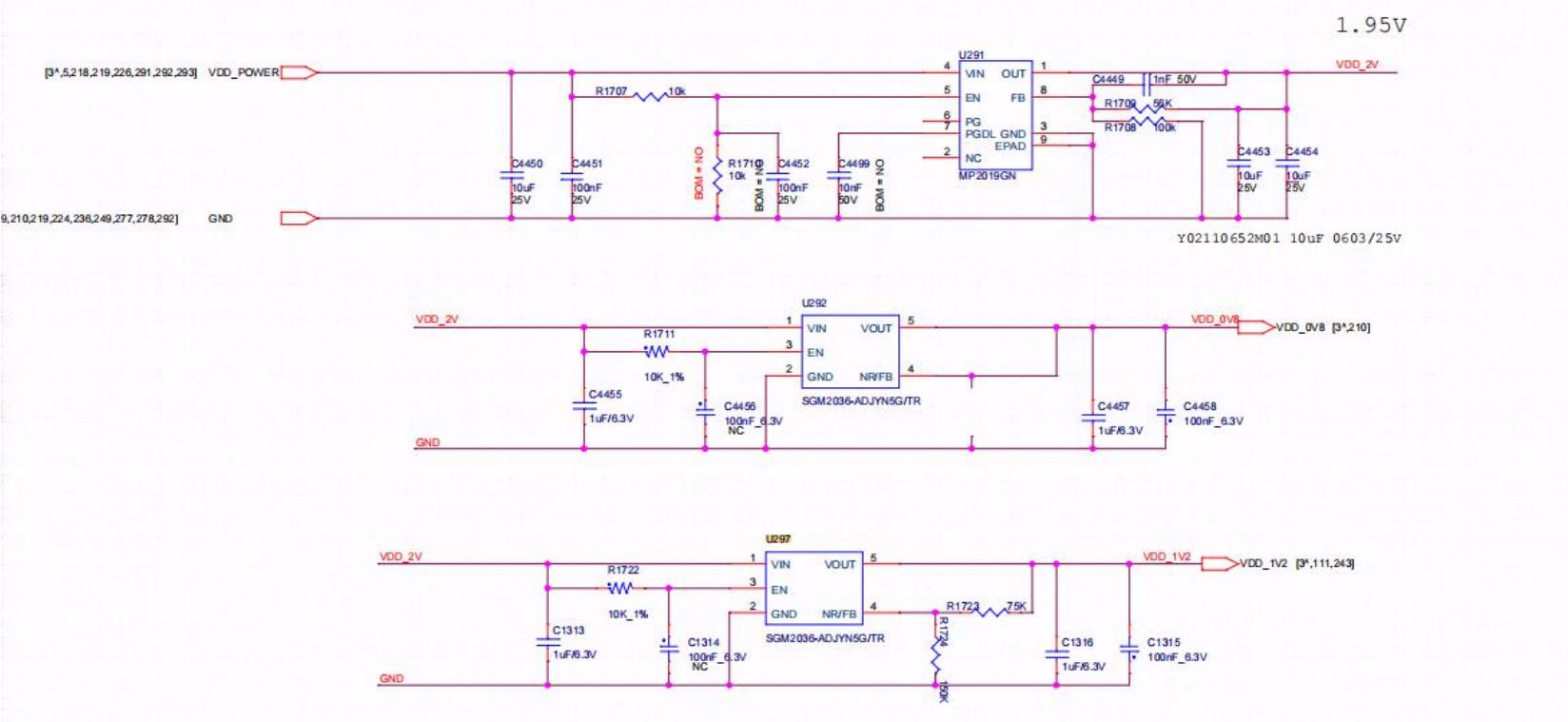
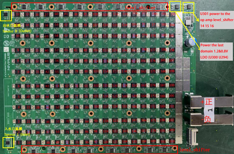
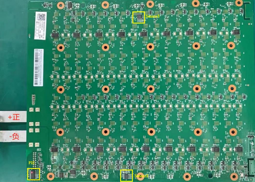
Figure 4-3
17 Domain direction note: Compared with 1362 and 1398, 1366 has canceled the MOS circuit and added 16 operational amplifiers. Starting from the second domain, addition operations on the signals.
Generally, if PT1&PT2 is defective or the connection between the two domains is defective, the op amp can be checked first, including abnormality of the 12M baud rate detection chip, etc. (The chip position in the PT2 test log starts counting from 0, asic 0 to 203. The voltage domain also starts counting from 0, that is, domain0 to domain16)
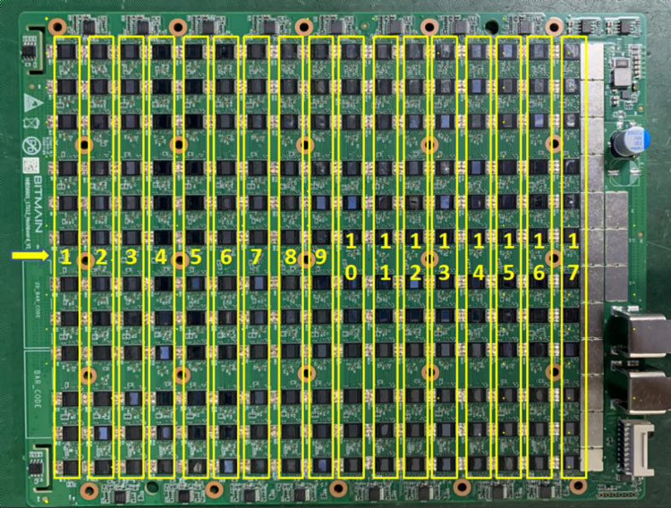
2. S19 XP Hyd. Hash Board Boost Circuit: The boost is supplied by the power source VDD_IN through U10 to convert to 25V, as shown in Figure 4-4.
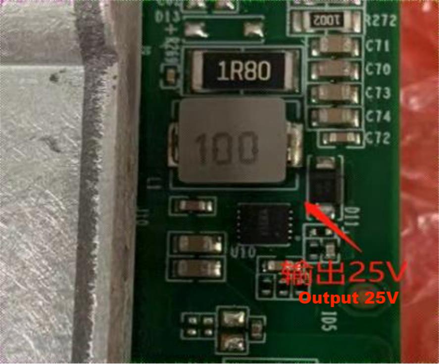
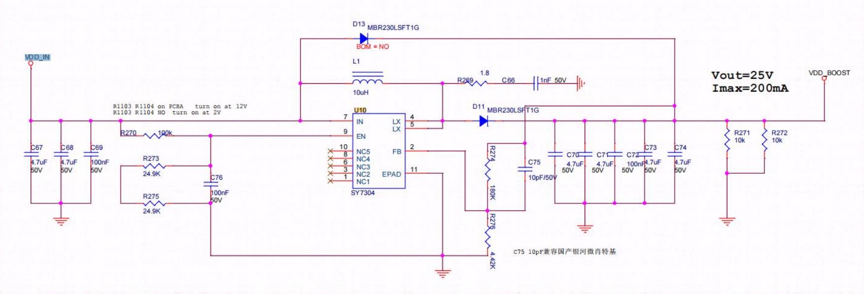
Figure 4-4
3. S19 XP Hyd. chip signal direction:
CLK signal direction: Generated by Y1 25M crystal oscillator. Y1 transmits from BM1 chip to BM204 chip, voltage is approximately 0.58-0.6V.
TX (CI, CO) signal direction: Enters from pin 7 of the IO interface (3.3V), passes through level conversion IC U2, and then transmits from BM1 chip to BM204 chip. Multimeter measures around 1.2V.
RX (RI, RO) signal direction: Transmits from BM204 chip towards BM1 chip, returns to signal cable terminal pin 8 via U1, and then back to the control board. Multimeter measures around 1.2V.
BO (BI, BO) signal direction: Transmits from BM1 chip to BM204 chip.
RST signal direction: Enters from pin 3 of the IO interface, passes through R216, and then transmits from BM1 chip to BM204 chip. Multimeter measures around 1.2V.
4. Complete machine architecture:
The complete machine primarily consists of 3 hash boards, 1 control board, and an APW111721a power supply, as shown in Figure 4-5.
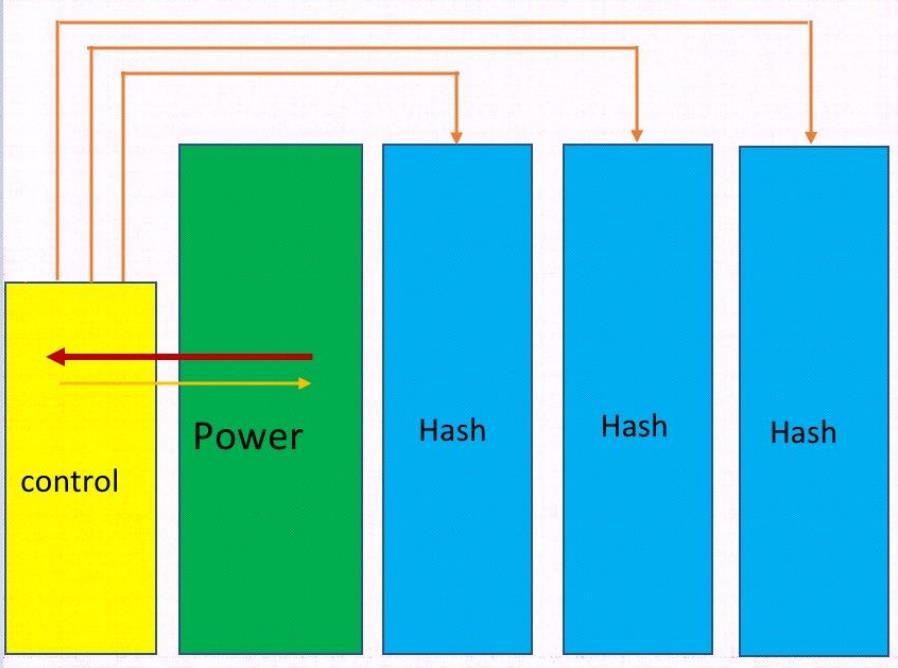
Figure 4-5
V. Common fault symptoms and troubleshooting steps for hash board
1. Phenomenon: Single board test detects 0 chips (PT1 station)
1) First, troubleshoot the power output, please refer to Figure 5-1.
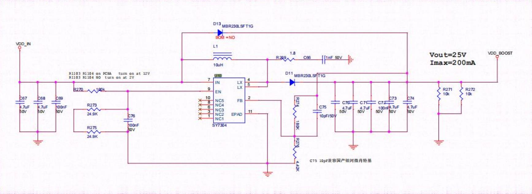
Figure 5-1
2) Check the voltage domain output.
Measure whether the domain voltage of about 1.2V is normal. If there is power supply at VDD_IN, there generally will be domain voltage. Prioritize measuring the output of the hash board power terminals.
3) Check the PIC circuit.
Measure whether there is an output at the second pin of U3, with a voltage of about 3.2V. If there is, continue to troubleshoot further. If there is no 3.3V, check that the test fixture ribbon cable is properly connected to the hash board and reprogram the PIC.
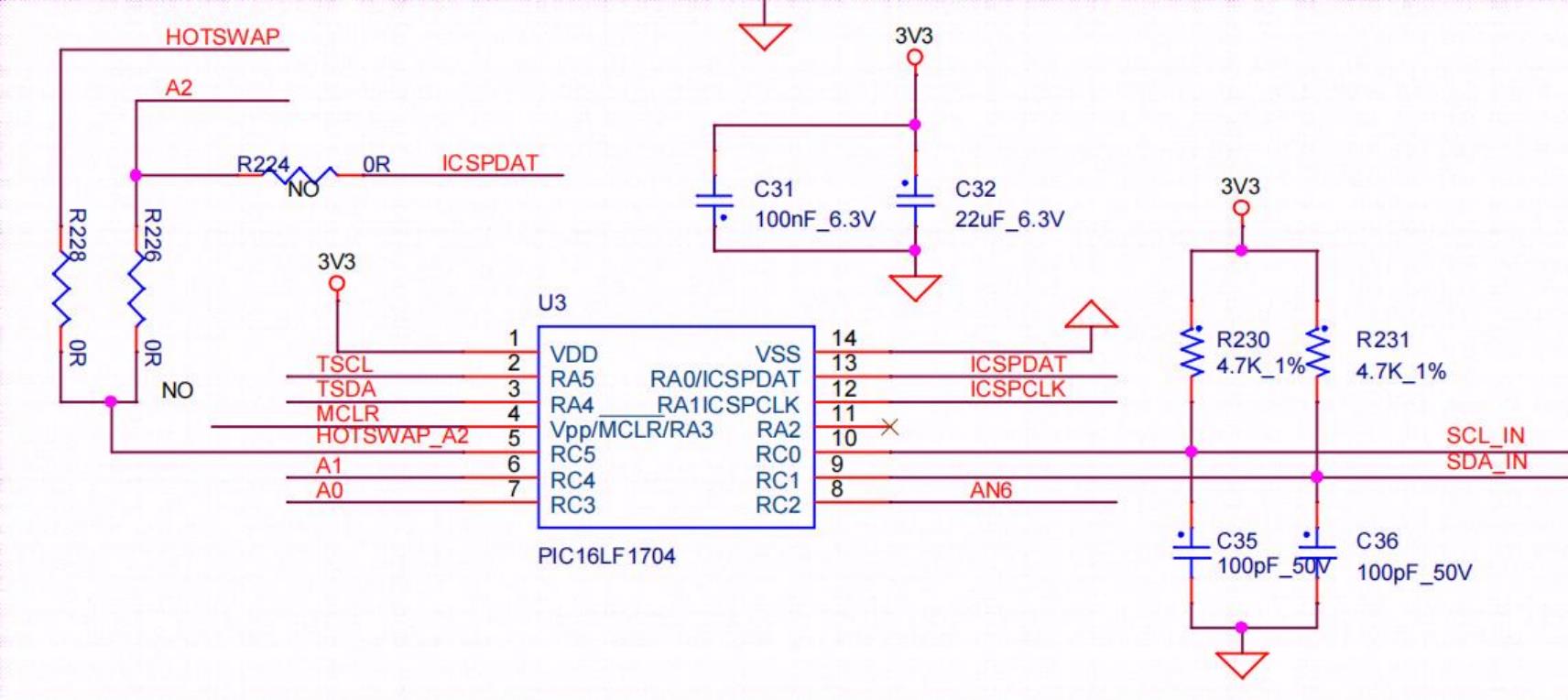
Figure 5-2
PIC programming steps:
(1) Programming of the computing board's PIC.
Program: PIC_H20_release_v101_4c54.hex
Download the programming tool: PICkit3. The pin 1 of PICkit3's ribbon cable corresponds to pin 1 of J2 on the PCB. It's necessary to connect pins 1, 2, 3, 4, 5, 6.
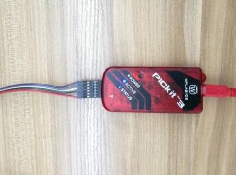
Figure 5-3
(2) Programming software:
Open MPLAB IPE, select the device: PIC16F1704, click on 'power' to choose the power supply method, then click on 'operate'.
First step: Select 'file' to find the .HEX file you want to program.
Second step: Click 'connect' to establish a normal connection.
Third step: Click the 'program' button, and after completion, click 'verify'. A prompt indicating verification completion signifies successful programming.

Figure 5-4
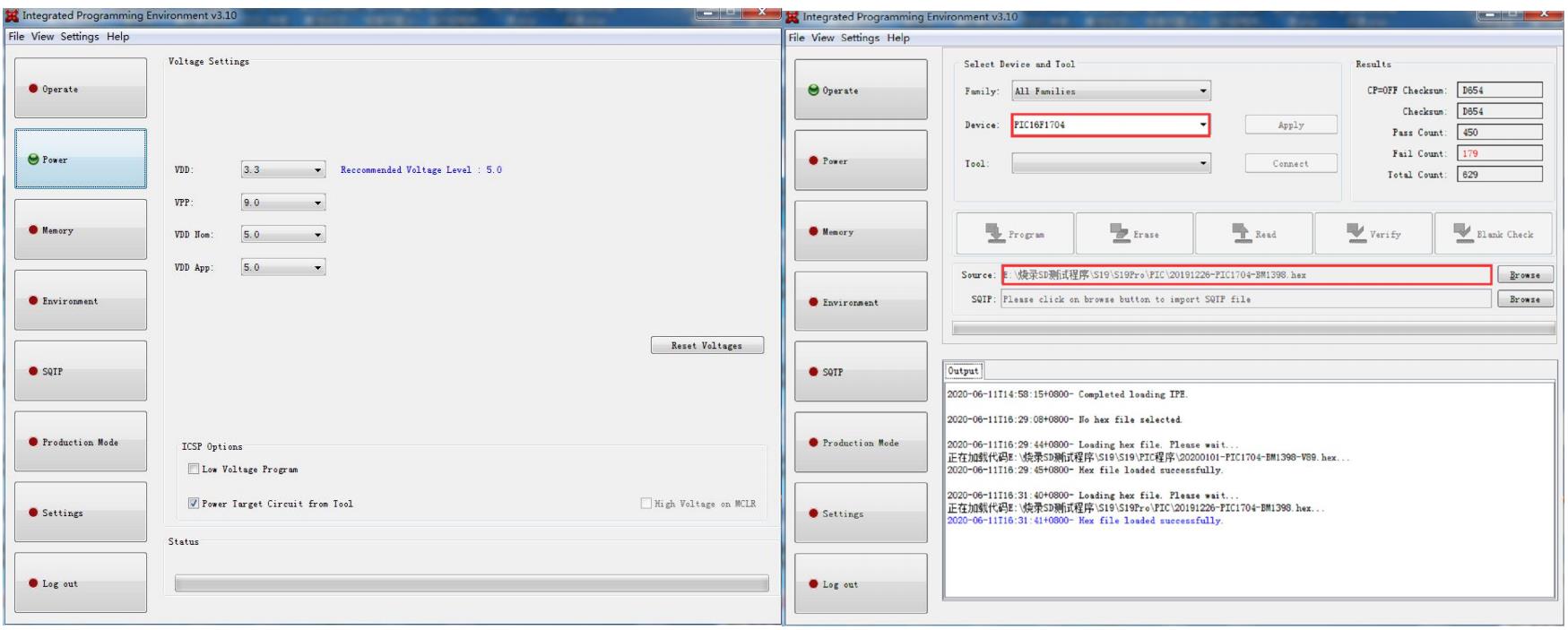
Figure 5-5
4) Check the output of each group's LDO 1.2V or PLL 0.8V.

Figure 5-6
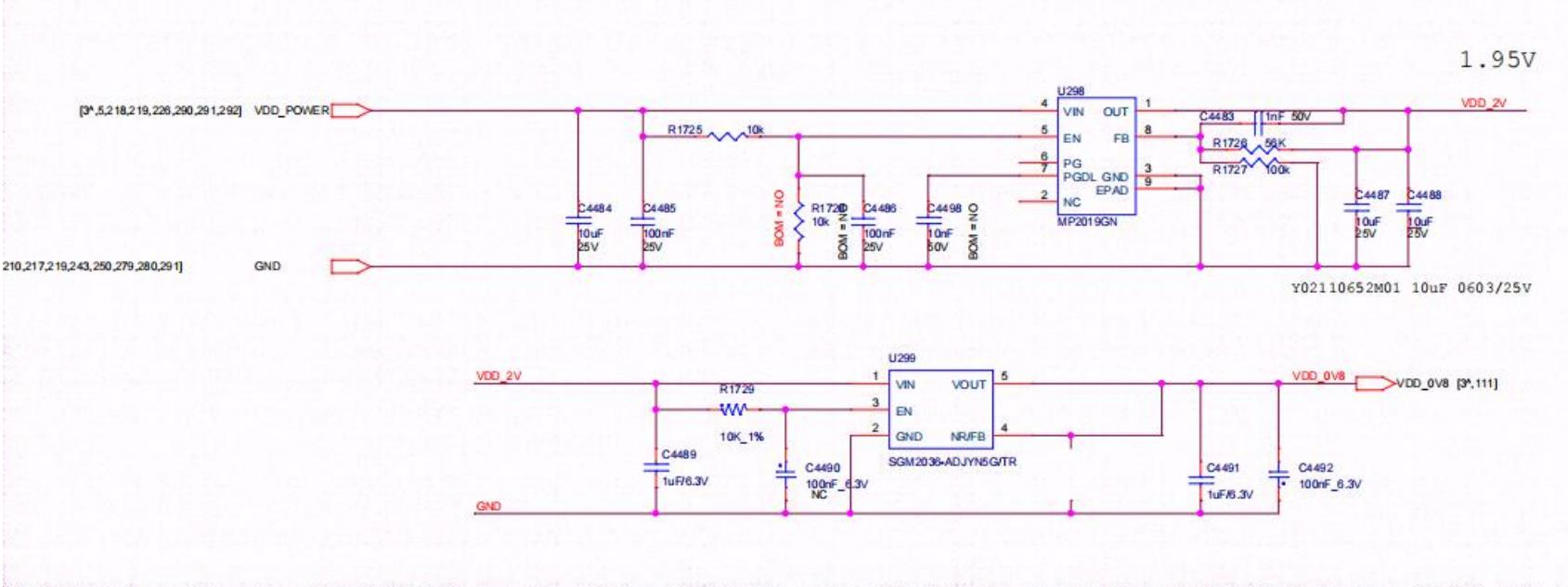
Figure 5-7
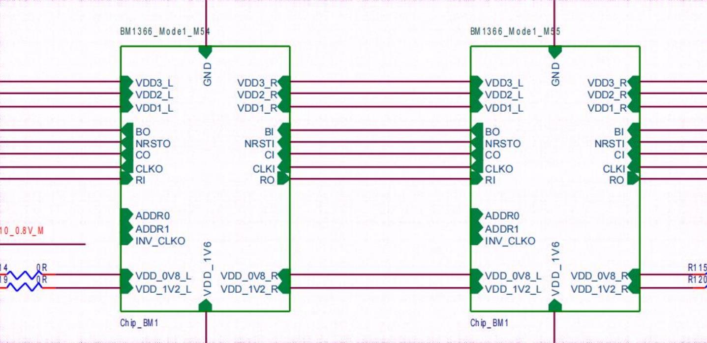
5) Check the chip signal output (CLK/CI/RI/BO/RST).
Refer to the voltage value range described in the signal direction description. If there is a significant deviation in the measured voltage values, compare them with the measurements of the adjacent group for determination.
2. When the EEPROM NG is displayed on the test fixture LCD screen, check whether U6 is soldered properly.
3. When the sensor NG is displayed on the test fixture LCD screen, indicating abnormal temperature readings, troubleshoot as follows:
A) Check the serial port log. If sensor=0, inspect the soldering of U4, R242, R243 chips or nearby SMD resistors and capacitors to see if they are normal.
B) Sensor={0, 1, 2, 3} corresponds to sensor positions at {U4, U5, U8, U7}. Refer to Figure 4-3 for the corresponding locations.

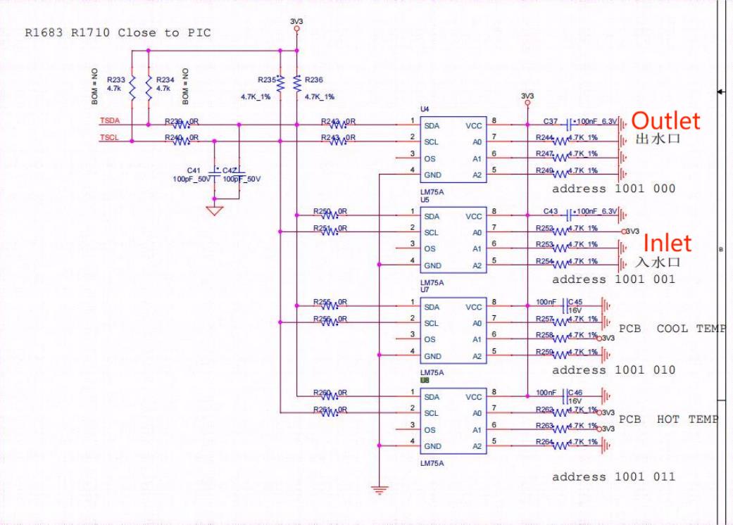
Figure 5-8
4. When the jig's LCD screen displays INIT NG WATER_TEMP, indicating abnormal readings of the water inlet and outlet temperatures, inspect whether U4, U5, and the SMD resistors and capacitors are soldered properly.
5. If the hash board's indicator light does not turn on, check whether the PIC's 3.3V is normal.
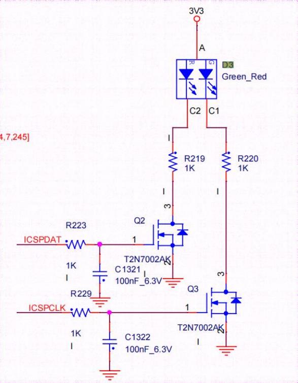
Figure 5-9
6. Phenomenon: Incomplete chip detection on the single board (PT1/PT2 stations)
a) LCD display ASIC NG: When it shows (0), first measure the total domain voltage of 21V and ensure the individual domain voltage is normal. Then, use a short-circuit probe to short the RO test point between the 1st and 2nd chips and the 1V2 test point, and then run the chip finding program. Observe the serial port log; if still 0 chips are found, it could be one of the following situations:
a-1) Measure the voltage at the 1V2 and 0V8 test points with a multimeter to see if it's 1.2V and 0.8V. If not, it might be an issue with the 1.2V or 0.8V LDO circuit in that domain, or the two ASIC chips in this domain might not be soldered well. Most often it's caused by a short-circuit in the 0.8V and 1.2V SMD filtering capacitors (measure the resistance of the relevant surface-mounted filtering capacitors on both sides of the PCBA), or check if the impedance to ground of the chip's VDDIO is abnormal. If abnormal, disconnect the VDDIO 1.2 & 0.8V resistors, two chips per group. If the impedance or diode measurement is still abnormal after disconnecting the resistors, then remove the corresponding chips.
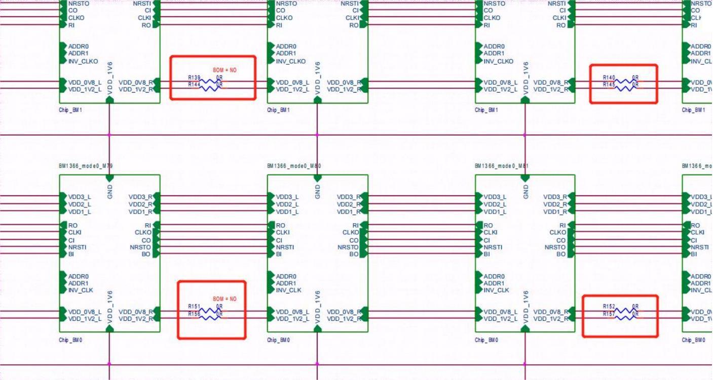
a-2) Check if there are any abnormalities in the U1 & U2 circuits, such as cold solder joints on resistors.
a-3) Once 1V2 and 0V8 are confirmed normal, sequentially measure if the RO, RST, CLK, CI, BI signals are normal.
a-4) Abnormal water temperature or cooling can lead to damage in U4, U5, or cause a short circuit to ground in the PIC chip U3. The first domain might have no 1.2V, 0.8V output, and chips BM1, BM2 might be damaged (U4, U5, U8, U7 damaged).
b) If in step a), 1 chip is found, it indicates that the 1st chip and the preceding circuit are fine. Use a similar method to inspect the subsequent chips. For example, short the 1V2 test point between the 38th and 39th chips and the RO test point. If the log finds 38 chips, then the first 38 chips are fine; if it still finds 0 chips, first check if that 1V2 is normal. If it is, then the issue is with the chips after the 38th. Continue using a binary search method to identify the problematic chip. Suppose the Nth chip is problematic, then shorting between the N-1 and N chips at 1V2 and RO finds N-1 chips, but shorting between the N and N+1 chips at 1V2 and RO does not find all chips.
c) LCD displays ASIC NG: (X, fixed report of a certain chip), there are two scenarios:
c-1) First scenario: The test time is about the same as for OK boards (usually, the value of X does not change in each test). The likelihood is that the problem is caused by abnormal soldering of the serial resistances of CLK, CI, BO before and after the Xth chip, so focus on these 6 resistors. A smaller probability is that one of the chips X-1, X, X+1 has abnormal soldering on certain pins.
c-2) Second scenario: If the appearance of the chip is normal, the voltage signal is normal, then it's an issue with the chip itself.
7. Phenomenon: Single board Pattern NG, i.e., incomplete response of nonce data (PT2 station).
Pattern NG is caused by significant differences in the characteristics of one chip compared to others, and several types of faults can cause it.
1) If chip die damage is found, simply replace that chip.
2) Chip bridging, cold soldering of chips (nonce response count of 0 or 1 for two chips in a domain).
3) The domain voltage in the domain is low, 1.2V & 0.8V voltages are normal, but there's an issue with the chip itself.
4) Multiple chips with nonce response count of 0, measure domain voltage, and troubleshoot starting from the domain with the low voltage.
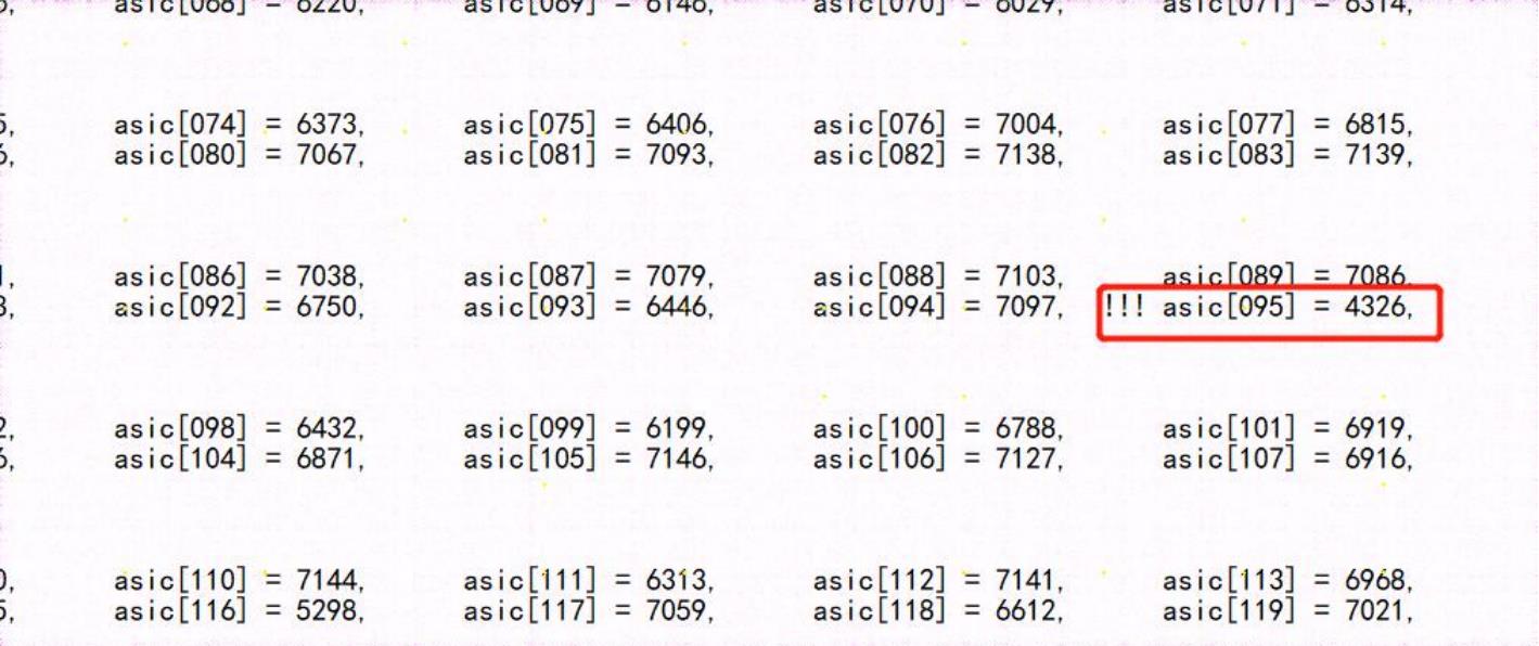
Figure 5-10
PS: It's important to note that both the domain and ASIC numbering start from 0.
8. Phenomenon: Chip testing is OK, but PT2 functional testing serial port does not stop (continuous running).
Repair method: During PT2 testing, observe the serial port print log. Generally, the issue is caused by a register address error in a certain chip. As shown in Figure 5-11, replacing the BM5 chip should resolve the issue (ASIC numbering starts from 0).
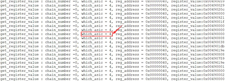
Figure 5-11
9. Phenomenon: PT1 chip testing is OK, but PT2 functional testing consistently reports a specific chip as NG.
Repair method: Inspect the appearance, measure the surface-mounted capacitors or resistors in front. Generally, the issue is caused by poor soldering of the chip or damage to a specific surface-mounted capacitor or resistor, abnormal resistance values, or a problem with the chip itself.
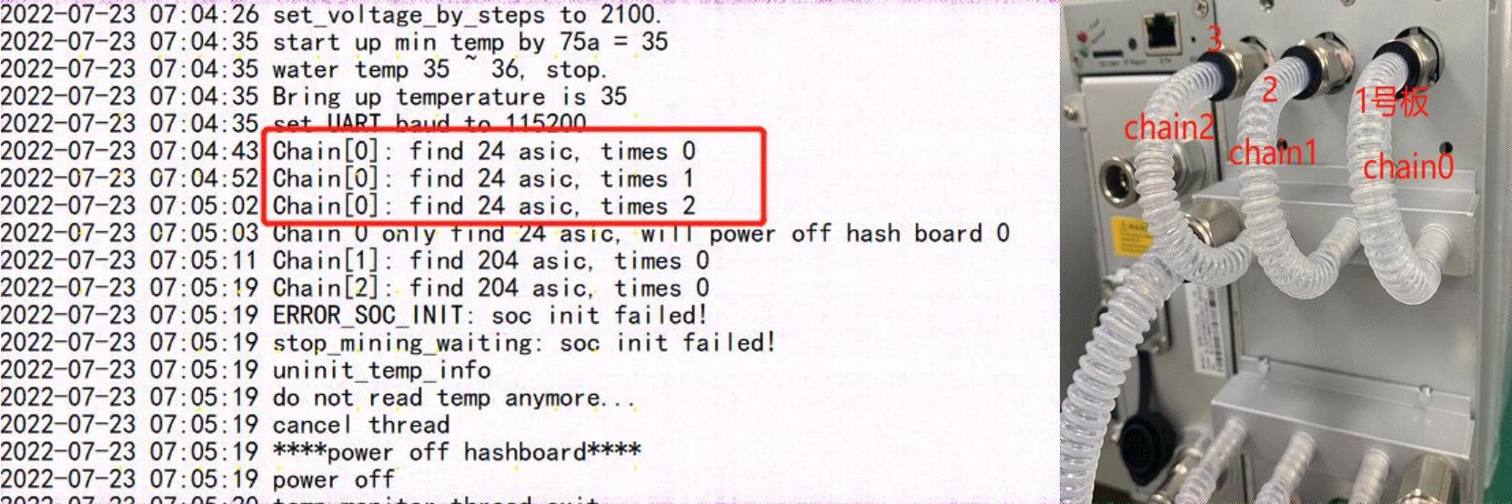
10. During the complete machine test, if R:1 is faulty and the log indicates "find x asic" (where x is less than 204), it means that not all chips on the hash board are being detected. Repair as per the PT1 chip testing anomalies. Chain0 represents the 1st hash board, and Chain2 represents the 3rd hash board. The hash board next to the power supply is the 3rd, Chain2. And the one in the middle is Chain1, representing the 2nd board.
VI. Control Board Issues Leading to the Following Problems
1. The complete machine does not run
1) Check if the voltages at several output points are normal. If there is a short circuit at 3.3V, first disconnect U8. If the short circuit persists, remove the CPU and then measure again. For other abnormal voltages, generally replace the corresponding voltage conversion IC.
2) If the voltages are normal, please check the soldering condition of the DDR/CPU.
3) Try updating the flash program using an SD card.
For machines flashed with a control board card to start normally, the following two steps are required:
a) After successful flashing, the green LED indicator should remain on. At this point, power off and restart.
b) After re-powering, wait for 30 seconds (the process of opening OTP).
OTP (One Time Programmable) is a type of memory in MCU, meaning it can be programmed only once: once the program is burned into the IC, it cannot be changed or erased again.
Precautions:
(1) If there is a sudden power cut during the OTP process or if the time is less than 30 seconds, it may cause the control board's OTP function to fail, resulting in the control board not starting (not connecting to the network). In this case, replace U1 (the main control IC FBGA on the control board). The replaced U1 should not be used again in the 19 series.
(2) For control boards with the OTP function activated, U1 should not be used in other series of machines.

Figure 6-1
2. The complete machine cannot find an IP address
The inability to find an IP address is likely due to operational anomalies. Refer to point 1 for troubleshooting.
Check the network port, network transformer T1, and the appearance and soldering of the CPU.
3. The complete machine cannot be upgraded
Check the network port, network transformer T1, and the appearance and soldering of the CPU.
4. The complete machine fails to read hash boards or has missing connections, reporting J:1
A. Check the condition of the ribbon cable connections.
B. Check the components corresponding to the chain on the control board.
C. Inspect the quality of wave soldering on the connector pins and the resistors around the connector interface.
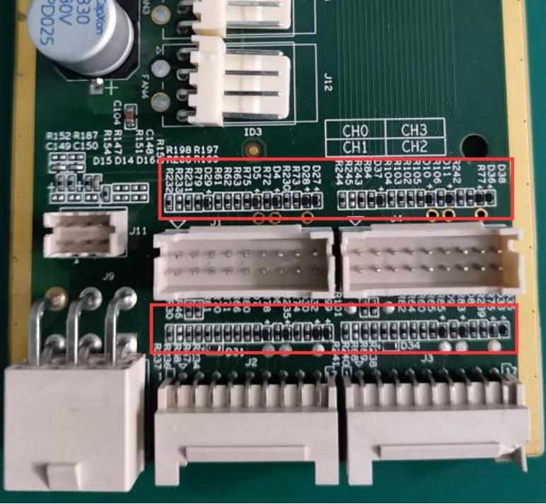
Figure 6-2
VII. Complete machine fault symptoms
1. Initial testing of the complete machine
Refer to the testing procedure document. Generally, problems that arise are due to assembly process issues or control board process issues.
Common symptoms include the inability to detect an IP and abnormal chain detection. If anomalies occur during testing, maintenance should be conducted according to the monitoring interface and test LOG indications. The methods for repairing during initial testing and aging testing of the complete machine are the same, and repairs should be made according to the corresponding abnormalities in the test items.
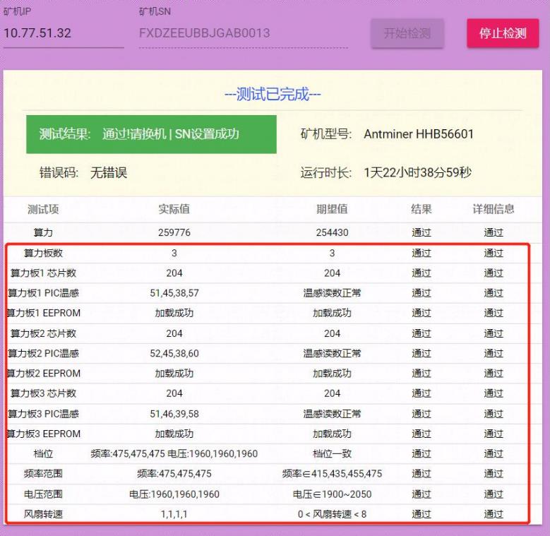
Figure 7-1
2. Aging Test: During the aging test, repairs should be based on the test conducted via the monitoring interface, for example:
1) Missing chain: Missing one out of three boards usually indicates an issue with the connection between the hash board and the control board. Check the ribbon cables for any open circuit issues. If the connection is OK, perform a PT2 test on the single board to see if it passes. If it does, it's likely an issue with the control board. If it doesn't pass, use the PT2 repair method.
2) Temperature anomaly: Generally, this refers to high temperatures. Our monitoring system sets a maximum PCB temperature of 80℃ for the machine, and the chip cannot exceed 95 degrees. If it exceeds this temperature, the machine will alarm and not work properly. Common causes include water outlet temperature exceeding 45 degrees or issues with thermal gel causing abnormal temperatures.
3) Inability to find all chips (OM firmware can boot and run, IM firmware cannot run, OM firmware's hash rate is 2/3 or 1/3 of the normal value): Check the log to see if the issue is insufficient chip count. If the chip count is insufficient, refer to the PT1 & PT2 tests for repairs.
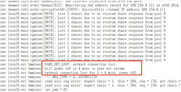
4) Loss of hash rate after running for a while, mining pool connection interrupted: Check the network.
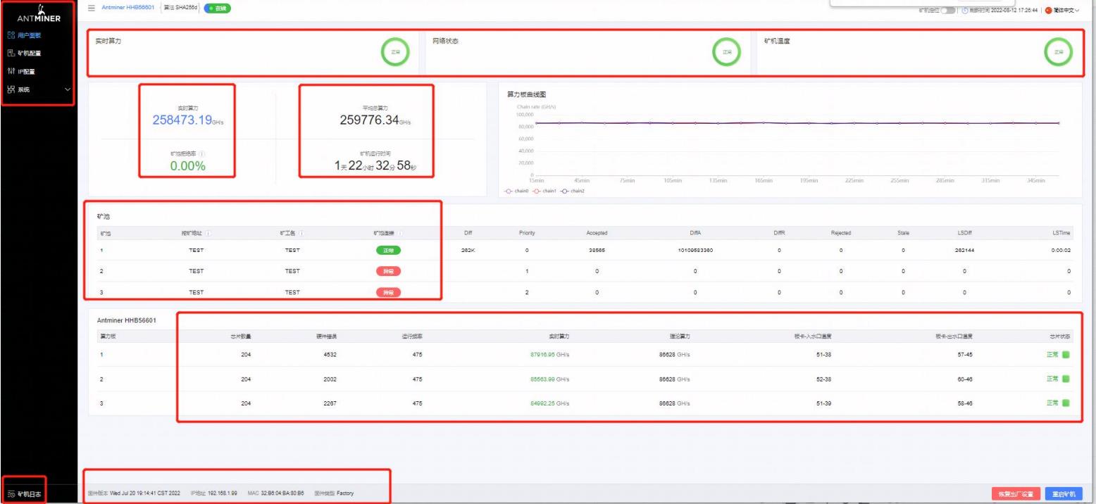
5) Aging test status of a normal, good quality machine.
6) The complete machine loses hash rate R:1:
For machines that pass single-board testing but show reduced hash rate when assembled for complete machine testing. For instance, as seen in the figure below, the first board loses its hash rate after about 3 minutes of operation. The specific analysis method is as follows: First, perform a single-board PT2 test to check if this board is OK. If the test fails to detect all chips, then repair the single board. If the test is OK in the normal range, then take out this board and run it separately with OM firmware, ensuring water inlet and outlet are connected. When the board drops out again, measure the domain voltage or signals like CLK, RO, etc. Generally, abnormalities can be detected, and then repairs can be made at the location of the anomaly.
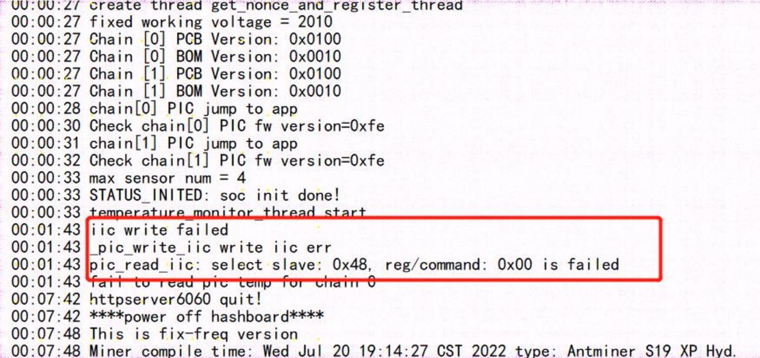
7) I2C error occurs during the operation of the complete machine, generally due to contact issues with the ribbon cable. Try restarting or re-plugging the ribbon cable.
3. After-sales and production repair water cooling test platform setup (Test water temperature: 30-35℃, single board water flow rate: 3-3.5L/min).
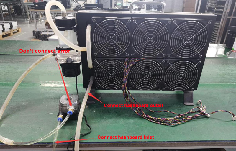
Figure 7-3

Figure 7-4
1) Since the first-generation water cooling system did not meet the requirements, an additional water pump needs to be added in series during the modification (or 2 water cooler rows connected in series).
2) Use 8mm air pipe joints and air pipes for the modification.
3) If the cooling does not meet the requirements, an air-cooling fan can be added for assistance.
VIII. Other Precautions
Repair Process Diagram

Figure 8-1 Repair flowchart
Routine Inspection: First, visually inspect the hash board to be repaired, checking for PCB deformation or signs of burning. If present, these must be addressed first. Look for obvious signs of burnt components, components that are displaced due to impact, or missing parts. Next, if there are no visual issues, start by checking the impedance in each voltage domain to detect any short circuits or open circuits. If any are found, they must be addressed first. Then, check if each domain's voltage is around 1.2V.
After passing routine inspection (generally, short circuit testing in routine inspection is essential to prevent burning out chips or other materials when powered on), use a testing jig to check the chips and make determinations based on the results. Based on the display results of the testing jig, start near the faulty chip and check the chip test points (CI/RST/RO/CLK/BI) and voltages like VDD0V8, VDD1V2, etc. Then, follow the signal direction, noting that the RO signal travels in reverse (from chip 204 to 1), while several other signals like CLK, CI, BI, RST travel forward (from 1 to 204), and locate the fault point through the power supply sequence.
When pinpointing the faulty chip, it needs to be re-soldered. Apply flux (preferably no-clean flux) around the chip and heat each solder point of the chip pins until they melt, allowing the chip pins to re-align with the pads and re-tin. If the problem persists after re-soldering, replace the chip directly.
After repairing the hash board, it must pass the testing jig test at least twice before being considered good. First, after replacing components and allowing the hash board to cool down, test it with the testing jig and set it aside to cool again. Second, after a few minutes when the hash board has completely cooled down, test it again.
After the hash board repair is OK, related repair/analysis records (repair report requirements: date, SN, PCB version, position number, cause of failure, responsibility for the defect, etc.) for feedback to production, after-sales, and R&D.
After recording, assemble it into a complete machine for routine aging.
For repaired hash boards and radiators, the thermal silicone grease must be reapplied.
Dear Customers,
Hello, May 1-5, 2026 (GMT+8) is China's May Day, and international logistics will be suspended. Our company will suspend shipments on the afternoon of April 30, 2026, and resume warehouse shipments on May 6 (GMT+8). We are deeply sorry for the inconvenience caused to you. Thank you for your trust and support.
Best wishes,
ZEUS MINING CO., LTD.