


IceRiver KS3 KS3L Hash Board Repair Guide
Ⅰ. Maintenance equipment requirements
1. Constant temperature soldering iron (350-400 degrees), used to flatten the residual tin slag on the pad's surface and reinforce the device.
2. A hot air gun is used for original mounting and soldering. Do not heat the PCB for a long time to avoid blistering it.
3. Multimeter, tweezers, electric screwdriver, temperature gun, short-circuit wire;
4. Solder wire, flux, board washing water, and tin-absorbing wire; board washing water is used to clean the soldering residue and appearance after maintenance.
5. Regulated power supply, fixed voltage 12V, current limit 4A (KS3), 2A (KS3L).
6. Auxiliary devices: high-temperature adhesive tape, heat dissipation paste
7. Common materials: quick-drying three-proof paint, 3600W power supply, data cable, power cable, 12038 cooling fan, control board, stepped spring screws, M4*10, three-combination hexagonal cross slot with pad, nickel-plated, M4*45, cross pan head screw, M3*10, cross pan head screw, M3*6.
Ⅱ. Operate requirements
1. Use a barcode scanner to record the whole machine SN code, PSU SN code, and the whole machine MAC address code. If the PSU is replaced, be sure to stick the whole machine SN code to the new PSU.
2. Upload the cause of the fault and the maintenance record.
3. After replacing any accessories, the PCB board should have no obvious deformation. Check whether there are missing parts, open circuits, or short circuits in the replaced parts and the surrounding areas. After the repair, the hash board must be tested more than twice and all must be OK before it can pass!
4. Check whether the maintenance tools and test tools (KS test fixture) can work properly.
5. If there are electrolytic capacitors or LED lights at the fault point, be sure to protect them with high-temperature tape to prevent damage to the capacitors.
6. When the hash board is powered on, pay attention to the fact that the negative power cable (black) must be powered on first, then the positive power cable (red), and finally the data cable. When disassembling, the order must be opposite to the installation order. First, remove the data cable, then the positive power cable (red), and finally, the negative power cable (black).
Note: The outer power terminal is the positive pole (+), and the terminal close to the plastic socket interface is the negative pole (-).
Ⅲ. Overall structure and principle
1. Working structure of KS3 and KS3L hash boards
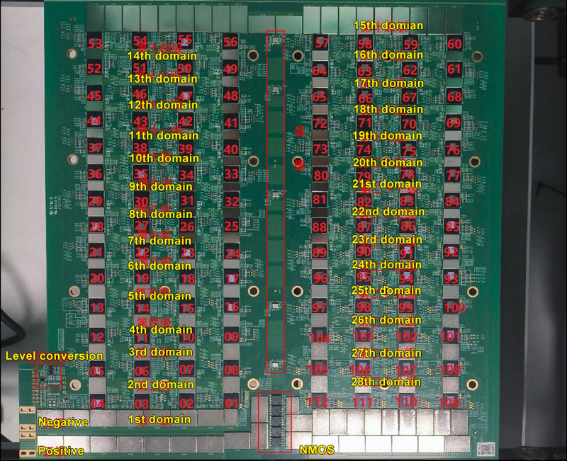
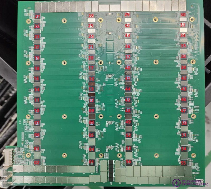
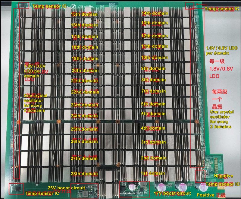
The hash board consists of 112 (KS3) / 56 (KS3L) ASIC chips, divided into 28 voltage domains, each containing 4 ASIC chips.
The ASIC chip working voltage of KS3 and KS3L is 0.4V during single-board testing. The boost circuit U15 provides the LDO powering of groups 28, 27, 26, 25, and 24 by outputting 15.5V (KS3) / 17V (KS3L) and then the LDO chip outputs 1.8V. The LDO powering of groups 23 - 1 is provided by 2.2V input voltage and then outputs 1.8V; all 0.8V is provided by the 1.8V of this domain through the LDO output.
2. KS3, KS3L hash board boost circuit
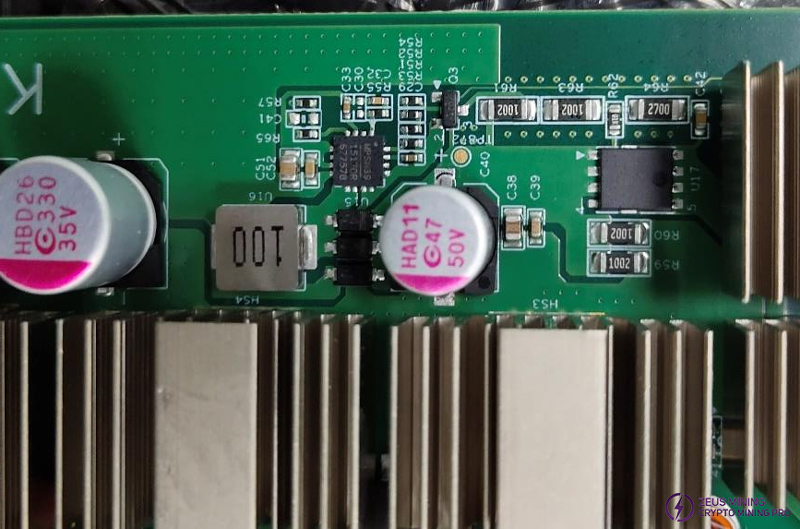
The boost powering is powered by the PSU 12V (KS3) / 15.5V (KS3L) to 15.5V (KS3) / 17V (KS3L).
3. Signal flow of KS3 and KS3L hash boards
Each two levels of the chip share a 25M crystal oscillator, and the normal voltage is 0.9V.
TX signal enters from IO port 7 pin (3.3V), passes through level conversion chip U8, and then transmits from chip 01 to chip 112 (KS3) / 56 (KS3L); when the signal flows normally, the voltage is 1.8V, and otherwise it is 0V.
The RX signal flows from chip 112 (KS3) / 56 (KS3L) to chip 01, and returns to the control board through the 8th pin of the IO interface after level conversion by U7; when the signal flows normally, the voltage is 1.8V, and in other cases it is 0V;
The RSTN signal flows from the 3rd pin of the IO port to the level conversion chip U6, and then passes through chip 01 to chip 112 (KS3) / 56 (KS3L) for transmission. The normal signal voltage is 1.8V.
4. Public powering
(1) Chip U15 (MP1517) 12V→15.5V/ 15.5V→17V
5. ASIC chip is powered by 3 sets of voltages
(1) ASIC chip domain voltage 0.40V;
(2) ASIC chip VDDPST/VDDPLL1V8 voltage (MP2019/SGM2036) 1.8V;
(3) ASIC chip VDD0P8/VDDPLL0V8 voltage (SGM2036) 0.8V.
Under normal working conditions, the normal voltage of the chip test point is:
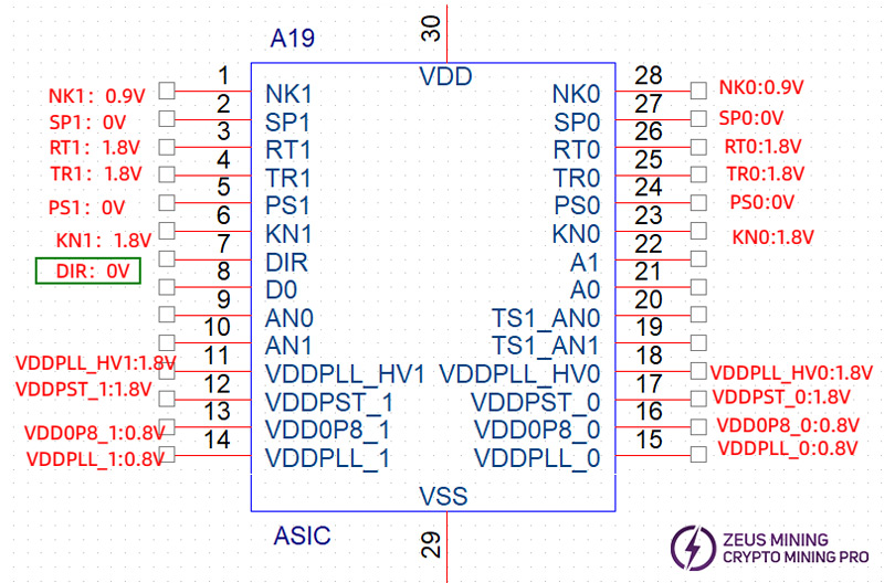
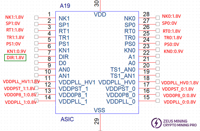
Since KS3 and KS3L are powered by voltage division, the pin voltage of each chip must be measured based on the "ground" of the current chip, and cannot be blindly based on the digital GND (0V).
IV. Normal single board test process of hash board
Step 1: Use a barcode scanner to record the barcode on the KS3 and KS3L machines and the QR code on the board, and make a record;
Step 2: Connect the interface board data cable and interface board power cable between the control board and the hash board, among them, the interface board power cable (yellow positive and black negative), the power terminal on the outside of the hash board is the positive pole (+), and the terminal close to the plastic socket interface is the negative pole (-), connect the negative pole first, then the positive pole.
Note: The interface data cable must be connected to the outermost interface.
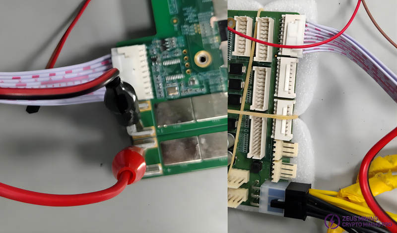
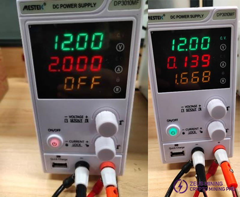
Step 3: Connect the network cable to the control board, make sure the power current limit is 12V@2A, and power on.
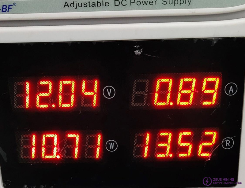
Step 4: At the moment of power-on, there is only about [email protected] current. At this time, only the control board is powered, and only U2, U3, U4, U5, U18, and U15 on the hash board are powered.
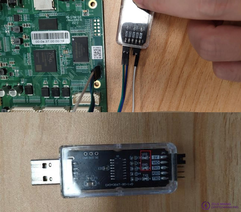
Step 5: (Serial port test method) Plug the serial port cable into the control board.
The blue and green wires are connected to the serial port cables respectively, and the white wire is connected to GND. After plugging into the computer, the red LED and blue LED in the red frame are always on, and the green LED outside the red frame will only flash when a command is entered. Click to here: How to use the KS tester to detect IceRiver hash boards?
Step 6: Automatically run the single board test program, at this time the enable is turned on and the current rises to about [email protected].
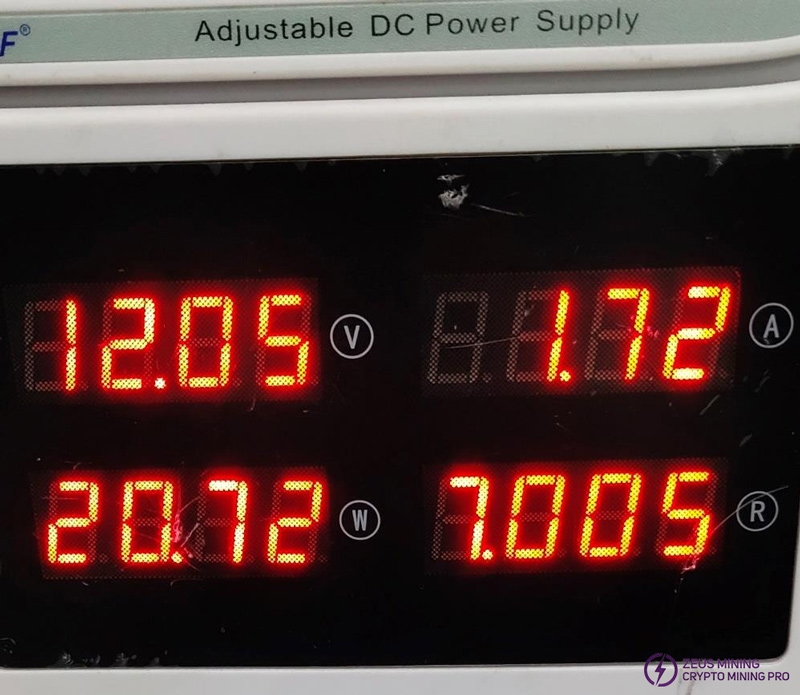
Step 7: While the program is running, the current rises to about [email protected].
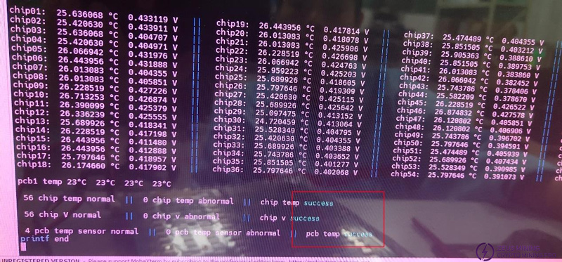
Step 8: After the program is finished, observe the results. The results show that the chip voltage and temperature, hash board temperature, and the number are consistent with the number of chips on the board, and three successes will pop up later, which is considered normal.
Ⅴ. Common bad phenomena and troubleshooting steps of hash board
The normal power-on current range of KS3 / KS3L single board is 0.9A, and the current range after the single board test program is running is 1.8A (KS3L), 3.8A (KS3). When verifying the board, the DC adjustable power supply configuration is: 12V voltage, 2A current limit.
1. Phenomenon: There is no abnormality in the 12V powering. After the program is running, the main voltage is always less than 12V.
Repair method:
Step 1: Check the front and rear voltages of the 12V main MOS chip to determine whether the MOS is turned on.


Step 2: Check the MOS enable voltage, use a multimeter to measure the T871 test point.
Step 3: Check if the Vg at U9 to U13 of the boost circuit is 22V (KS3) / 26V (KS3L).
Use a multimeter to measure the voltage at T873, and the voltage before and after R34.

Step 4: Check whether the voltage of U18 is normal, including whether Vin, Vout, Ven, and Vfb are normal. Among them, Ven=0V and Vfb=0.6V are considered normal.
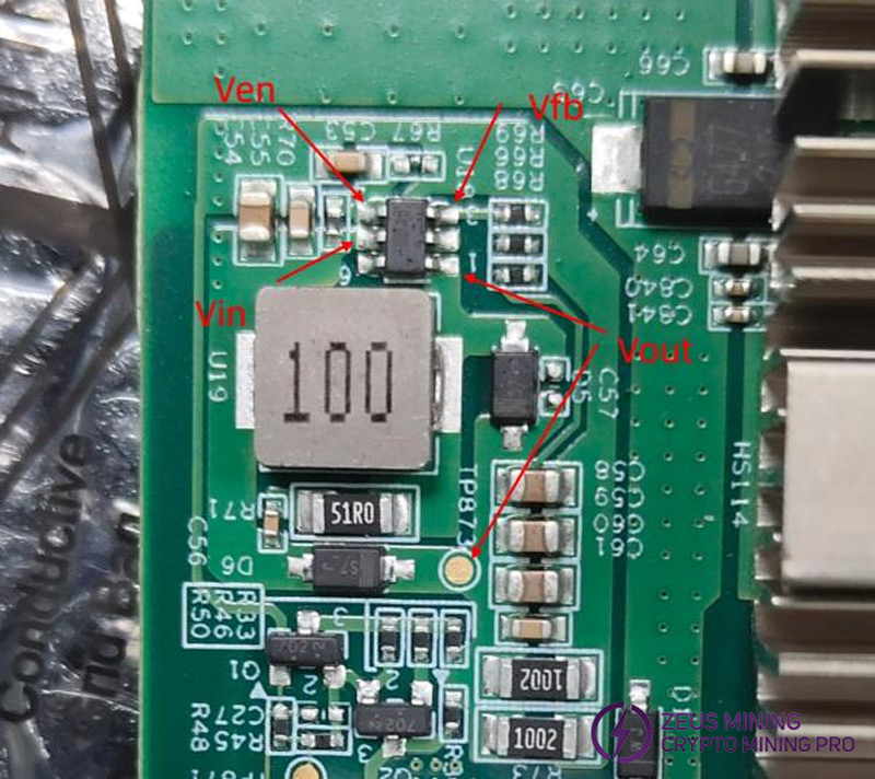
2. Phenomenon: The 12V powering voltage is fine, but the number of chips is insufficient, 0 or garbled.
Solution:
Method 1:
Step 1: Measure whether the voltage before and after the MOS tube is around 12V.
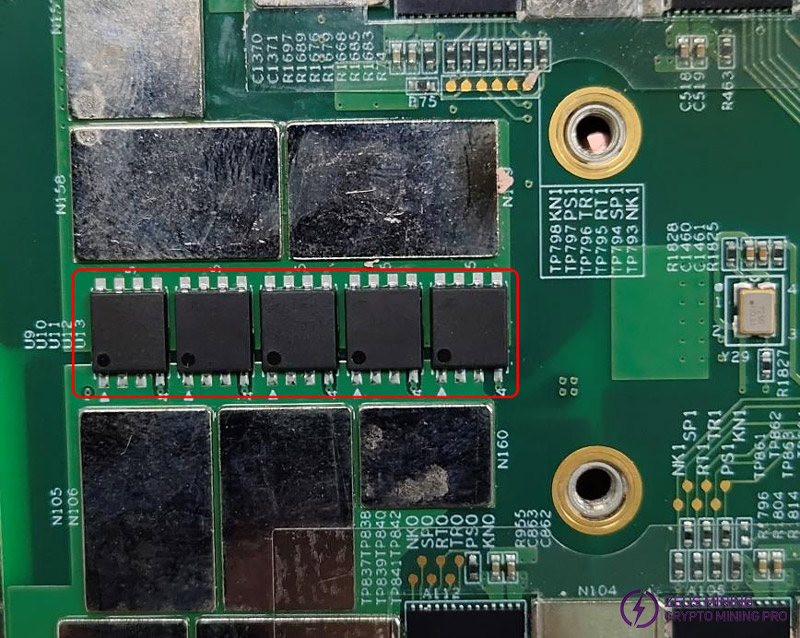
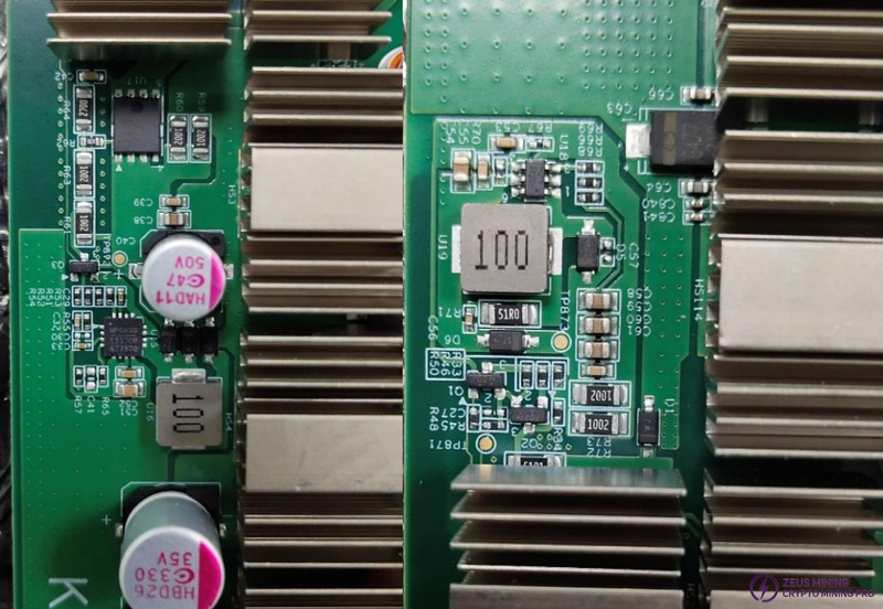
Step 2: Measure whether the two boost circuits are within the normal range by testing TP872 15.5V (KS3) / 17V (KS3L), TP873 22V (KS3) / 26V (KS3L). The left picture is TP872, and the right picture is TP873.
Step 3: Check whether the voltage of each group of chips is greater than 0V. If the voltage is near 0V, it is considered that the chip in the current voltage domain has a short circuit.
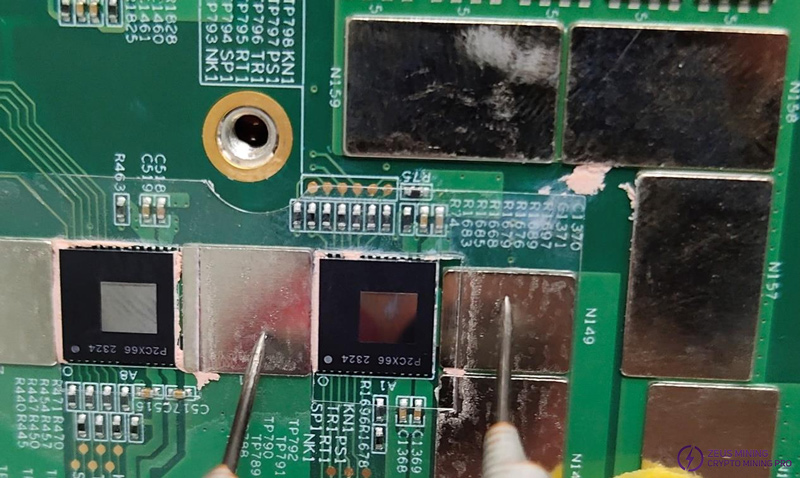
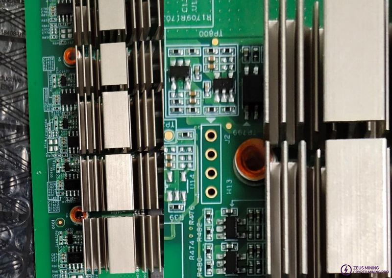
Step 4: Check whether the 1.8V and 0.8V of each chip are normal. If the 1.8V or 0.8V voltage of the chip is abnormal, it is necessary to determine the voltage point of each chip and determine the output status of 1.8V-LDO and 0.8V-LDO.
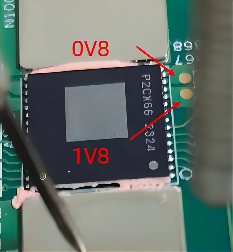
The left picture shows a high-voltage LDO, which is used for 1.8V powering of domains 28, 27, 26, 25, and 24. The rest are ordinary LDOs, which are used for powering of domains 1 to 23 and 0.8V powering of domains 28, 27, 26, 25, and 24.
When running the single board test program, we can determine the voltage at the chip pin, or resistance to judge whether the chip is normal.
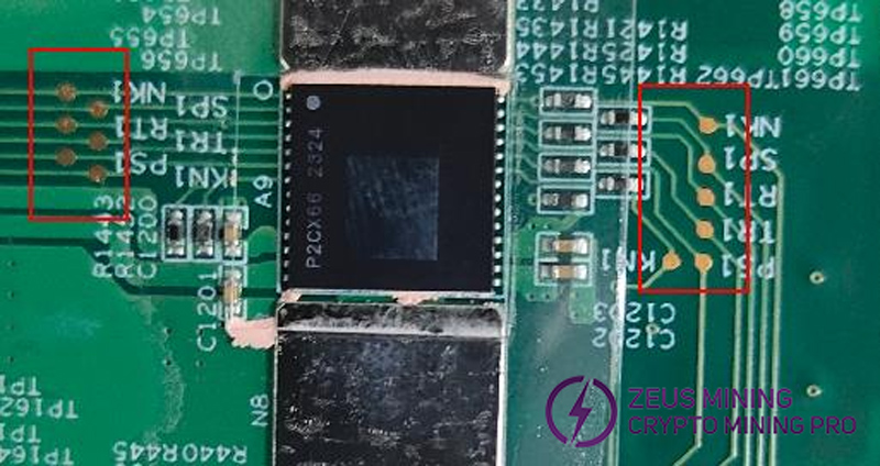
Test point-test point | Resistance |
DIR voltage = 1.8V | |
NK1-NK1 | About 2KΩ |
SP1-SP1 | About 7~12MΩ |
RT1-RT1 | About 12KΩ (chips 1~4 are about 0.4MΩ) |
TR1-TR1 | About 15MΩ (chips 1~4 are about 40MΩ) |
PS1-PS1 | About 7~12MΩ |
KN1-KN1 | About 13MΩ |
DIR voltage = 0V | |
NK1-NK1 | About 13MΩ |
SP1-SP1 | About 7~12MΩ |
RT1-RT1 | About 15MΩ |
TR1-TR1 | About 12KΩ |
PS1-PS1 | About 7~12MΩ |
KN1-KN1 | About 2KΩ |
Step 5: Check the voltage of each group of chip pins to the "ground" of the current voltage domain.


Method 2:
The detection method of the first four steps is the same as that of method 1, and there are differences afterwards.
Step 5: Keep the hash board running the single-board program and use a multimeter to measure the level at the DIR of the ASIC chip. The measurement results are generally two types: Vdir=1.8V / 0V.
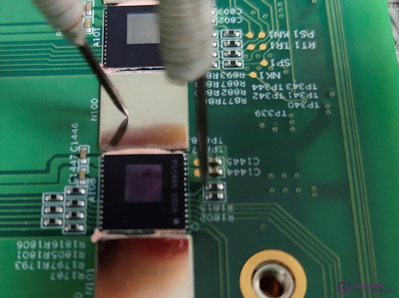
Step 6: Use a short-circuit wire according to the test results in step 1.
Vdir=1.8V: Use a short-circuit wire to pull up the PS0 pin of the ASIC chip. Note that the pull-up voltage can only be 1.8V.
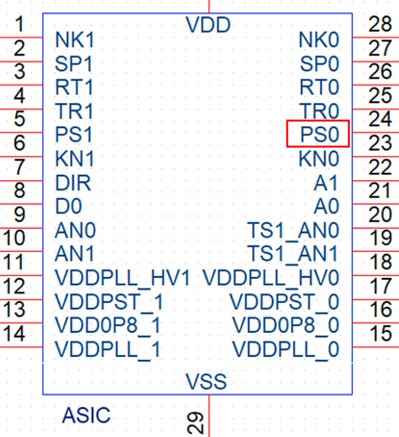
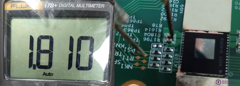
Vdir=0V: Use a shorting wire to pull up the SP1 pin of the ASIC chip. Note that the pull-up voltage can only be 1.8V.
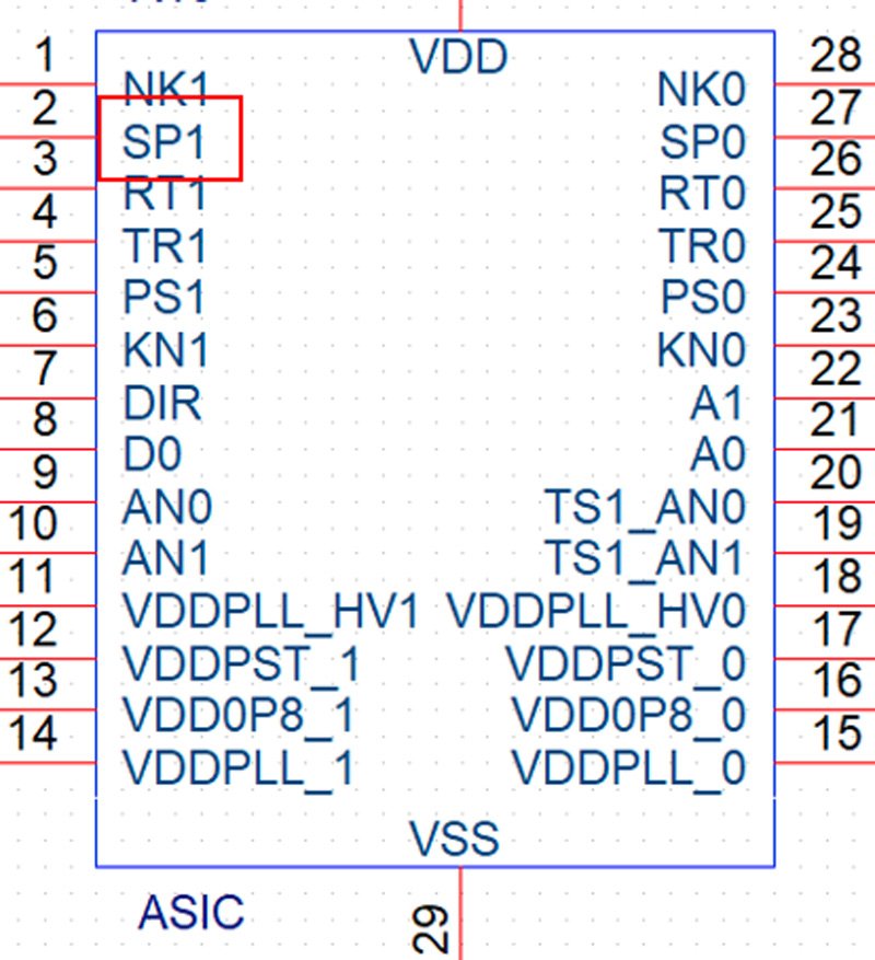

Step 7: Continue to observe the results of the single board test program to see if the chip is still garbled. If it is still garbled, we need to repeat steps 5 to 7 one level higher until no garbled code is generated. In this case, it is determined that the previous chip of the current chip is abnormal. After replacing it, run the single board program to verify!
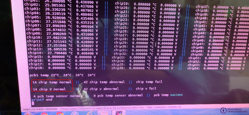
Step 8: As shown in the figure above, when the voltage at DIR is measured to be 1.8V, the PS0 voltage is pulled up. At this time, the single-board program automatically terminates when it reaches the 14th chip, proving that there is no abnormality in the first 14 chips. At this time, it is necessary to continue to check backwards and pull up the PS0/SP1 signal on the voltage of the next voltage domain until the problematic chip is found.
VI. Common faults of the whole machine and troubleshooting steps
1. Power consumption comparison table of the whole machine:
Model | Version | PSU model | Voltage | Power consumption |
KS3 | All versions have the same power consumption | 12V | 3200W | |
KS3L | sy0811_ks3L_miner/sy0808_v2_ks3L_miner | BP-H-3640 | 14V | 2700W |
KS3L | sy0811_ks3L_miner | AP276 | 13.5V | 2550W |
KS3L | sy0808_v2_ks3L_miner | AP276 | 13V | 2410W |
2. Phenomenon: The power consumption of the whole machine cannot reach the power consumption in the above comparison table and the web backend cannot be logged in.
Solution:
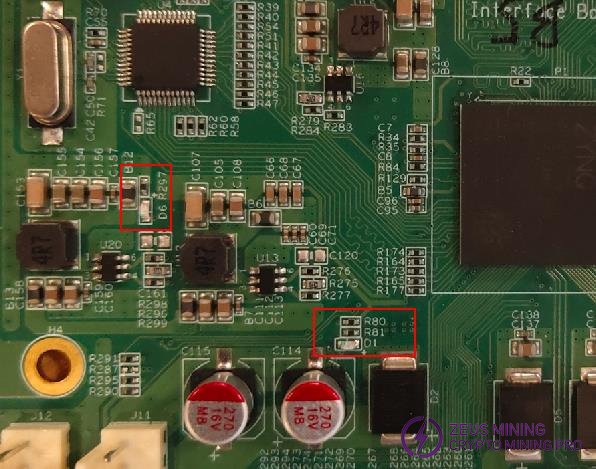
Step 1: Check whether the two blue LEDs (position numbers: D1, D6) on the control board are on.
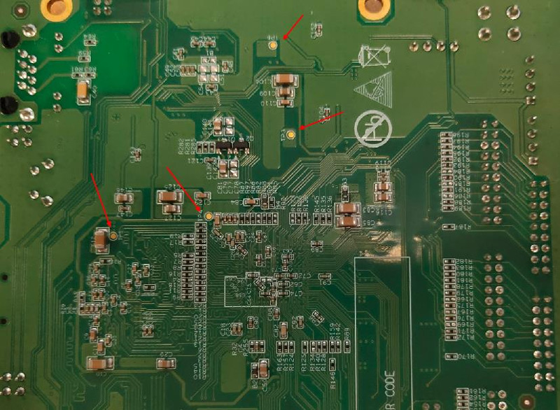
Step 2: Check whether TP3, TP4, TP5, and TP6 on the control board are: 1.0V, 1.8V, 1.5V, and 3.3V respectively.
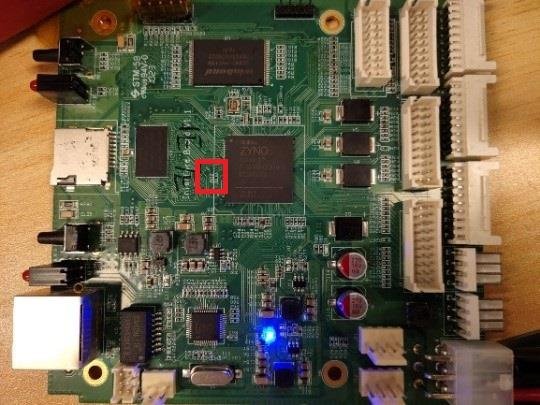
Step 3: If the above voltages are normal, and one of the blue LED lights (position number: D6) is on, and the current is about 0.08~0.1A, it means that the system has not started. We need to check SOC, DDR, and FLASH, and measure the voltage on both sides of the R22 resistor, as shown in the figure below. When the voltage on both sides is about 1.5V, it may be that the program in the FLASH is abnormal or the FLASH is damaged; when the measured voltage is about 0.69V, it means that the FLASH and SOC are normal. If you cannot enter the system at this time, there is a high probability that the DDR is abnormal. Exceeding this current means that there is a short-circuited components in the circuit.
VII. Usage method for the test program
Step 1: Use the control board with the maintenance program;
Step 2: Connect the control board, data cable and hash board. First connect the negative cable (black) to the power terminal inside the board, and then connect the positive cable (red) to the power terminal outside the board. After the connection is successful, press the DC adjustable PSU switch;
Step 3: Print the voltage and temperature information of the current ASIC chip on the hashboard on the serial port tool. Only when the number is consistent with the actual number of chips on the board and the temperature and voltage are normal can the whole machine be installed for hashing test.
Ⅷ. KS3, KS3L installation
Step 1: Use board cleaning water and air pump to clean the hash board that has passed the single board test.
Step 2: Replace the insulation film and spray the three-proof coating on both sides of the LDO chips on the hash board.
Step 3: Apply thermal paste and install the heat sink. The thermal paste must accurately cover the center area of the chip.
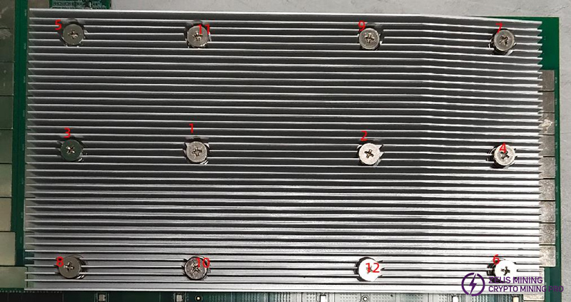
Step 4: Put an insulating gasket on the end of the stepped screw, adjust the torque to 9, and screw in the order shown in the numbers on the picture from small to large.

Step 5: Plug the power cord and data cable into the control board.
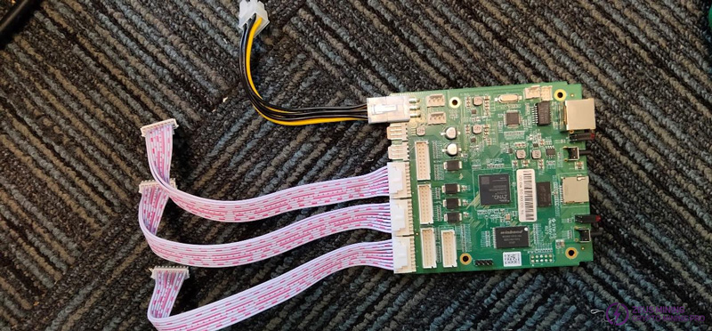
Step 6: Insert the hash board vertically into the chassis. KS3 and KS3L both have 3 hash boards.
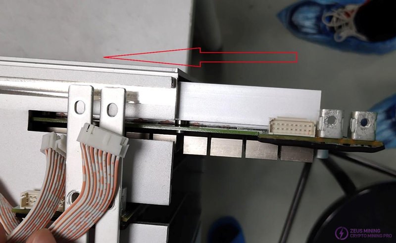
Step 7: Insert the 3600W PSU parallel to the side of the chassis.
Step 8: Insert the control board parallel to the top of the chassis.
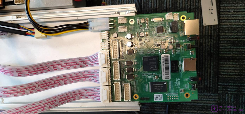
Step 9: Connect the conductive copper sheet to the 3600W PSU and hash board, adjust the torque to 9, and connect the interface board power cord to the conductive copper sheet together, paying attention to the positive yellow and the negative black.

Note: The yellow and black wires should be connected to the conductive copper sheet as shown in the picture. Do not connect them in reverse or short circuit. The six screws connecting the conductive copper sheet and the hash board must be tightened. There are also 6 screws fixing the conductive copper sheet to the PSU.
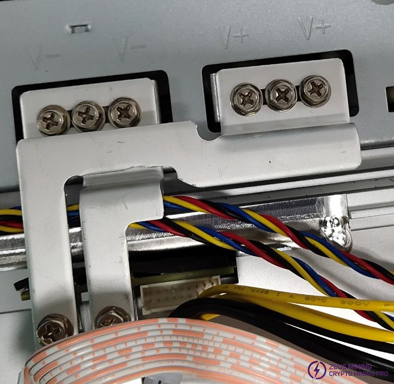
The above 12 screws use: M4*10, three-combination hexagonal cross slot with pad, nickel-plated.
Step 10: Connect the data cable to the hash board, and the four fans and PSU IIC must be connected to the hash board.
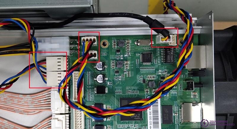
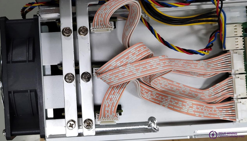
The connection sequence between the power board and the control board must be consistent with the diagram.
Step 11: Cover the chassis top cover, side cover, power cover, and fan, and adjust the torque to 9.
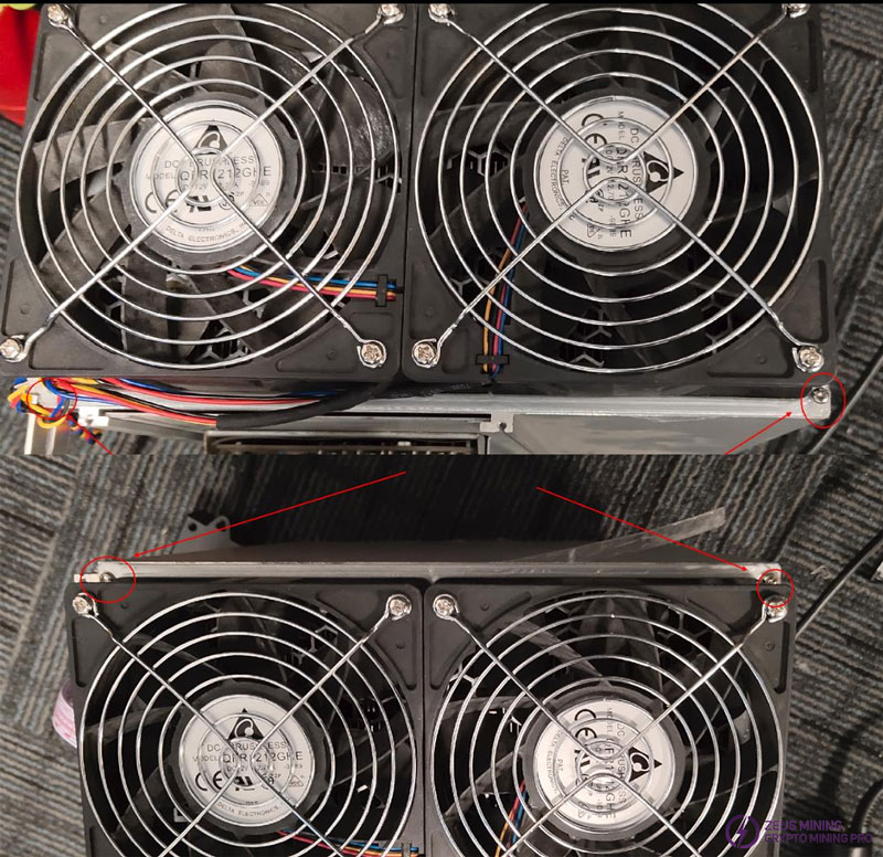
Notice: a fan is fixed with 4 screws, and the screws must be driven diagonally. The screws used to fix the fan net are: M4*45, cross head, and NYLOK.
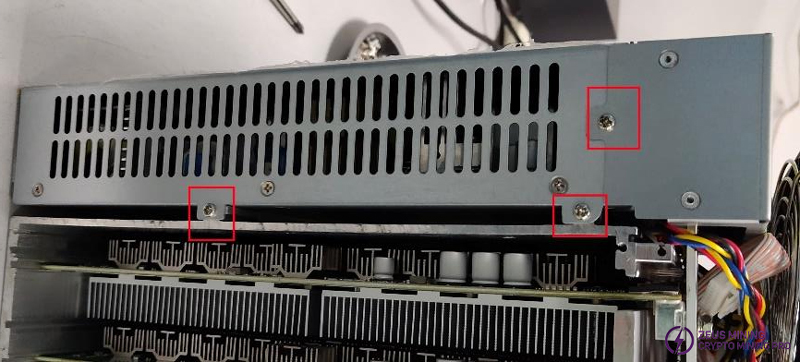
There are 3 screws behind the power board.
The screws used to fix the fan and power cover are: M3*10, cross head, NYLOK.
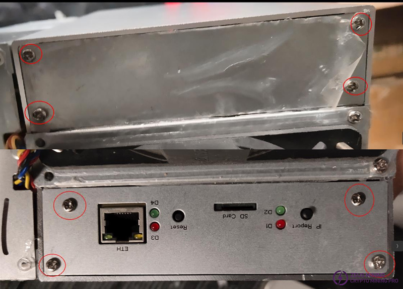
As shown in the figure, the front and rear panels need 4 screws each, and the screws used are: M3*6, cross pan head*3, M3*6, cross countersunk head*1.
Step 12: Connect the power, network cable, and use the group control software to scan and connect to the machine in the current network segment.
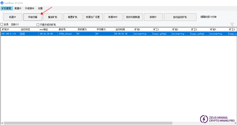
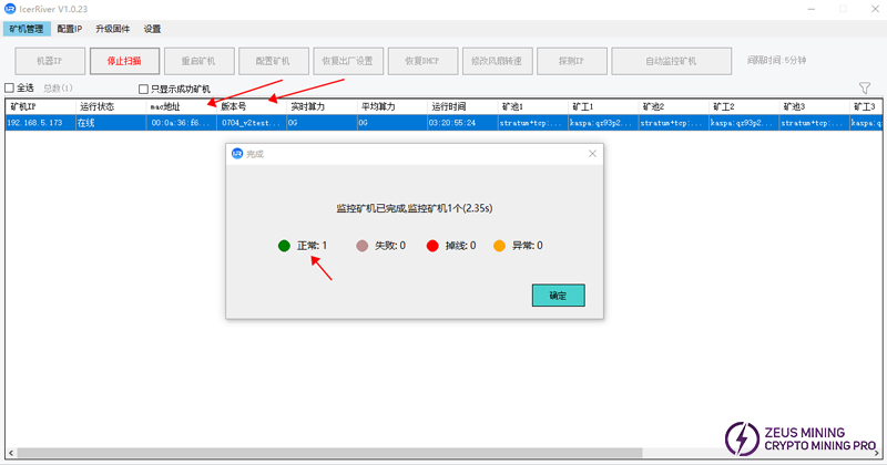
When the test software scans the MAC address and version number, it means that the current machine is officially connected to the local area network. At this time, enter the miner IP in the browser address bar to enter the Web background.

Step 13: Enter the Web background to check whether the hashrate meets the standard and whether the fan and board temperature are normal.
Name:admin
Password:12345678
KS3 reaches 8TH/s hashrate within 10~15 minutes of startup, and KS3L reaches 5TH/s hashrate, which is considered normal.
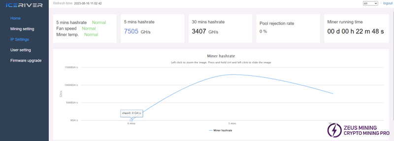
As shown in the figure, we can see the hash rate and temperature status of each board, and at the same time see if Fan speed and Miner temp are displayed as Normal. The fan speed of the whole machine is within 6000±10% is considered normal.

Ⅸ. Other precautions
1. Conventional maintenance process
(1) Observe the appearance
(2) Measure the impedance
(3) Power on and measure the voltage
(4) Power on and test
(5) Determine the fault based on the detection information
(6) Locate the fault and re-solder it first before replacing it
(7) Perform aging test after multiple tests after repair
2. Conventional inspection: First, visually inspect the hash board to be repaired to see if there is any deformation or burning of the PCB. If so, it must be processed first; whether there are obvious signs of burning of parts, parts impact displacement or missing parts, etc.; secondly, after visual inspection, the impedance of each voltage domain can be tested to detect whether there is a short circuit or open circuit. If found, it must be processed first. Thirdly, check whether the voltage of each part is normal.
3. Conventional short circuit detection is necessary to avoid burning chips or other materials due to short circuit when power is on.
4. Unless necessary, generally do not operate the ASIC. If it is determined that the ASIC has failed, it must be powered off. If necessary, remove the corresponding power chip.
5. After the repair is completed, clean the tin slag on the surface of the board and power it on/install it for testing after it cools down naturally.
Dear Customers,
Hello, May 1-5, 2026 (GMT+8) is China's May Day, and international logistics will be suspended. Our company will suspend shipments on the afternoon of April 30, 2026, and resume warehouse shipments on May 6 (GMT+8). We are deeply sorry for the inconvenience caused to you. Thank you for your trust and support.
Best wishes,
ZEUS MINING CO., LTD.