


Antminer S21+ (Plus) Hydro Hash Board Repair Guide
S21+ hydro Product Specifications Reference
Miner specifications | S21 hyd. (HHB68501) | S21 hyd. (HHB68501) | S21 hyd. (HHB68501) | |
Power consumption on the wall @35℃ W | 5360±5% | 5070±5% | 4785±5% | 5691±5% |
Operating frequency MHz | 410 | 601 | 566 | |
Hash rate of the whole miner T | 355 | 338 | 319 | |
APW power supply model | APW111721 Three-phase, copper busbar + screws | APW111721 Three-phase, copper busbar + screws | APW111721 Three-phase, copper busbar + screws | |
Miner size mm | 339.2 * 176 * 208 | 339.2 * 176 * 208 | 339.2 * 176 * 208 | 339.2 * 176 * 208 |
Number of chips in the whole miner | 648 | 285 | 480 | 473 |
Number of hash boards in the whole miner | 3 | 3 | 3 | 3 |
Hash board chip matrix | 18*12 | 19*5 | 20*8 | |
Miner weight (including packaging, kg) | 14.8 | 14.8 | 13.6 | |
I. Repair Platform/Tool/Equipment Preparation Requirements
1. Platform Requirements:
Anti-static mat repair workbench (workbench must be grounded), anti-static wrist strap and grounding.
2. Equipment Requirements:
Constant temperature soldering iron (350℃-380℃), fine tip for soldering SMD resistors/capacitors, etc.;
Hot air gun: the temperature is 350±10℃;
Multimeter: equipped with soldering needle tip covered with heat shrink tubing for easy measurement (recommend Fluke);
Oscilloscope: recommend RIGOL DHO814 100MHz digital oscilloscope;
Network cable: connect to Internet, stable network.
3. Repair Test Tool Requirements:
(1) APW11 power supply. APW111721 calibrated for power must be used for SWEEP testing. Power adapter cable DIY: Use thick copper cable (recommend 4AWG, length <60cm) to connect power supply positive and negative pole to the hash board for power; Use 19-series universal test fixture, fixture base package version B047 (P/N: ZJ0001000004).
(2) PT1 test supports APW9, APW9+, APW11 power supplies.
4. Repair Auxiliary Materials/Tool Requirements:
Solder paste Senju M705, flux, PCB cleaner plus anhydrous alcohol; PCB cleaner for cleaning flux residue after repair; Use thermal gel for application on chip surface after repair; Reballing stencil (8mm x 8mm chip size), desoldering braid; When replacing a new chip, the chip pins must be tinned before soldering to the hash board. Apply thermal gel evenly on the chip surface before securing the liquid cooling plate.
(1) Barcode scanner
(2) RS232/TTL converter board 3.3V
(3) Prepare or make your own short-circuit probe
5. Common Repair Spare Parts Requirements:
SMD Resistor, 33, OHM, 1%, 1/20W, R0201 (0603);
SMD Resistor RES, 10K, +/-1%, 1/16W, 0402;
SMD Resistor Res 0 ohm, 1/16W 0402 5%;
SMD Ceramic Cap, 1uF, +/-10%, 16V, X5R, 0402;
SMD Ceramic Cap, 1UF, 6.3V, 20%, X5R, C0201 (0603);
SMD Ceramic Cap Cap, 22uF, +/-20%, 6.3V, X5R, 0603.
II. Repair Requirements
1. Pay attention to workmanship when replacing chips. After replacing any component, the PCB should show no obvious deformation. Check the replaced part and surrounding areas for missing parts, open circuits, or shorts.
2. Repair personnel must possess basic electronic knowledge, at least one year of repair experience, and be proficient in BGA/QFN/LGA package soldering techniques.
3. After repair, the hash board must be tested OK at least twice before passing. Each work order has a corresponding number of hash board SNs; each board SN is unique and cannot be reused during test scanning.
4. Check tools and test fixtures to ensure they function correctly. Confirm the repair station test software parameters, test fixture version, etc.
5. Testing after chip replacement: First perform chip detection (pass required) before functional testing. Functional testing must ensure the liquid cooling plate assembly is OK. When installing the liquid cooling plate, thermal gel must be applied evenly on the chip surface, and the cooling fan must be at full speed or connected to a liquid cooling radiator and water block. When using a water block for heat dissipation, add a water pump at the inlet to increase flow rate.
CAUTION: Testing PT1 without a heatsink will cause chip overheating and hash board burnout.
6. When measuring signals during PT1 chip detection, the heatsink MUST be secured, otherwise it will cause hashboard burnout. PT3 testing requires connection to a water block, with a water flow rate of 2-3L/min, and water temperature between 32-35℃. Testing cannot proceed below or above this temperature range.
7. When measuring signals and voltages with the heatsink secured, measurements can be taken on the BOT side. The bottom bracket has reserved openings for accessing signal and voltage test points.
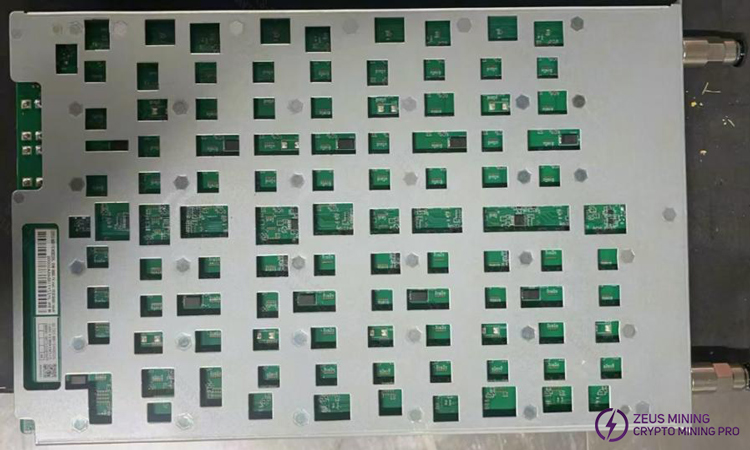
8. When replacing a new chip, print solder paste on the pads and ensure the chip is pre-tinned before soldering to the PCBA for repair.
9. Test fixtures at the repair end all use Test_Mode and barcode scanning mode for testing. After passing the test, the production end is streamlined from the first test station, and the normal installation and aging (mount into machine of the same level).
10. For PCBA that had the heatsink removed, after successful repair, the liquid cooling plate MUST be re-applied with thermal gel before re-installation and line testing (otherwise, it will cause long-term running failures in the whole miner).
III. Test fixture Manufacturing and Precautions
The tester should meet liquid cooling heat dissipation for hash board and facilitate signal measurement.
1. Obtain P/N: ZJ0001000004 test fixture, flash the corresponding fixture base package.
2. For first use of H6HB70701 series test fixture, update the fixture control board FPGA using the SD card program. Extract the files to the SD card, insert the card into the fixture slot; power on for about 1 minute, wait for the control board indicator to flash twice 3 times indicating update completion. (Failure to update B047 base package will cause inability to test, reporting failures).


3. Prepare the test SD card as needed. For PT1 chip detection, PT1&PT3 combined functional test, simply extract the compressed package to make the SD card; no need to modify configuration files. The PT1 test card is used for SMT sampling inspection and repair of faulty single boards. (Repaired boards MUST follow the production flow starting from PT1 again. Repair personnel must not skip testing stations).
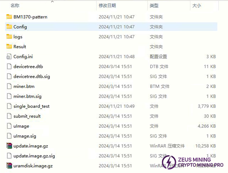
4. For production, after-sales, and external repair ends, PT1 chip detection testing requires a barcode scanner, serial port tool, and network cable.
IV. Principle Overview
1. H6HB70701 Hash Board Working Structure:
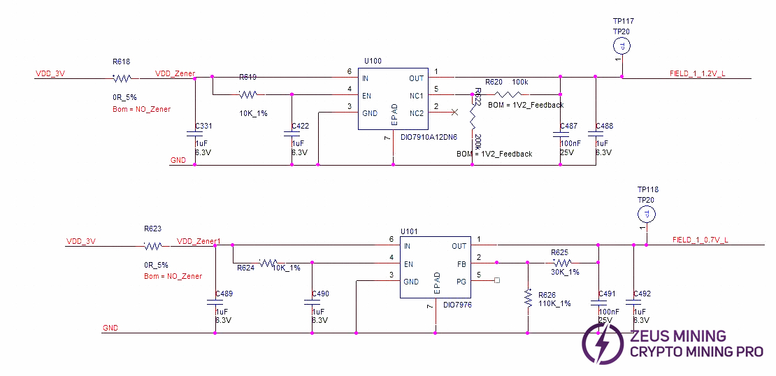
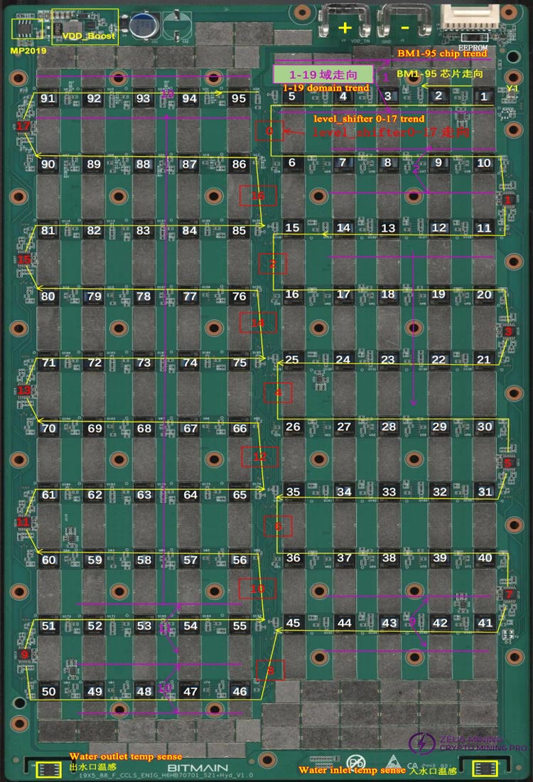
The hash board consists of 95 BM1370 chips (PCB silkscreen order BM1-BM95), divided into 19 groups (domains), each domain consisting of 5 ASICs. The chip domain operating voltage is approximately 1.05V. Domains 1-17 chip VDDIO is powered by 1.2V & 0.7V LDO chips. Each domain uses 2 LDOs (one LDO outputs 1.2V, one outputs 0.7V). Note: LDO chip inputs are taken from cross-domain voltage.
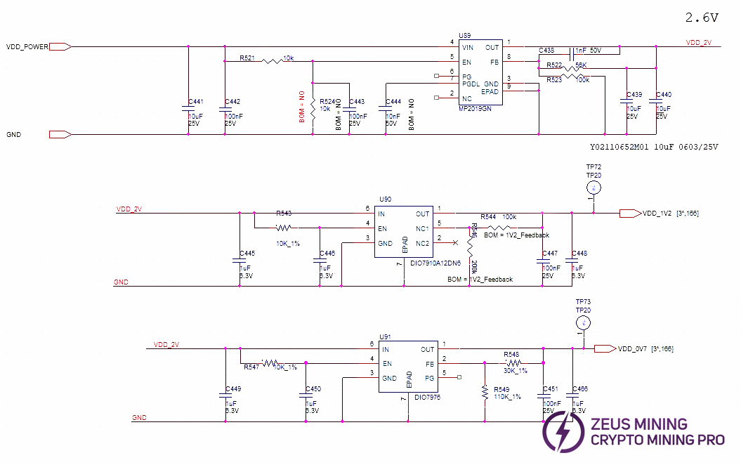
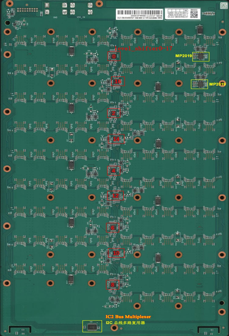
Domains 18 and 19 (high voltage domains): Each domain is powered by one MP2019 (U82, U89) outputting 2V to supply the LDOs, which then power the chip VDDIO. Specifically, LDOs U87 and U88 (1.2V & 0.7V) are powered by MP2019 U82. LDOs U90 and U91 (1.2V & 0.7V) are powered by MP2019 U89. See diagram below.
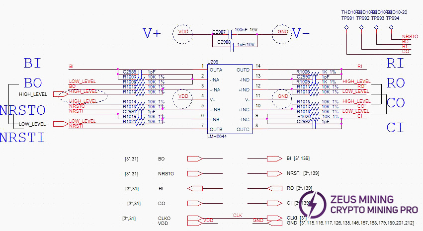
Compared to other models, the S21+ Hyd. hash board changes LDOs to low thermal resistance types and adds 18 level_shifter ICs to perform addition operations on chip-related signals.
From the second domain to the last, a total of 18 level_shifter ICs are used.
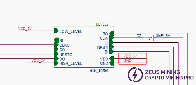
The power supply of level_shifter 0 and 1 is 6V & GND.
The power supply of level_shifter 2 - 15 uses cross-6-domain 6V (e.g., level_shifter 3 takes voltage from domain 6, 7V-1VGND, and so on).
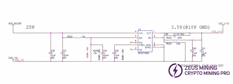
And Level_shifter 16 & 17 are powered by the VDD_21.5V output from U3 MP2019. See diagram below.
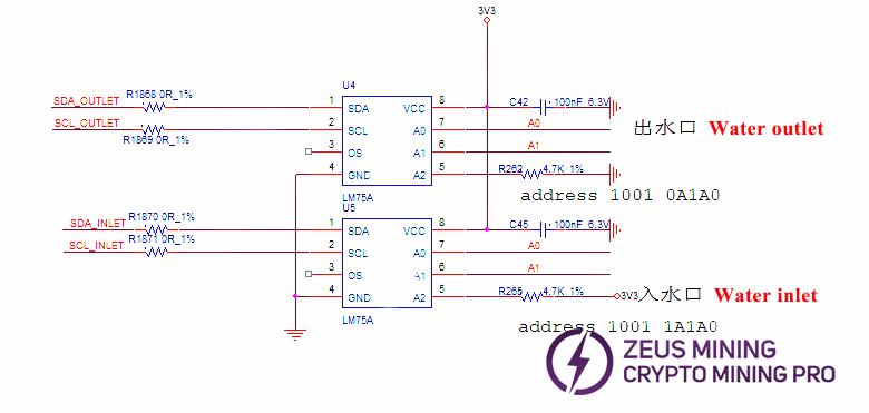
Temperature sensing circuit uses 2 LM75A sensors, one at water inlet, one at water outlet, powered by the control board's 3.3V via the ribbon cable.
Hash board 20 domain layout (Chip position in PT3 test log starts counting from 0: asic 0-94; voltage domains also start from 0: domain0-domain18).
Note: Compared to 1362 and 1398, 1370P cancels MOS and PIC circuits, adds 18 operational amplifiers, and performs addition operation on signals starting from the second domain.
If the PT1&PT3 test fails, or there is a problem at the junction of the 2 domains, we can first check the op amp, including the 12M baud rate chip detection abnormality, etc., we can first check the op amp.
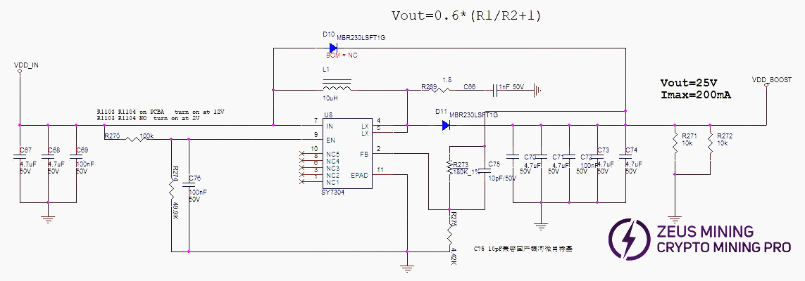
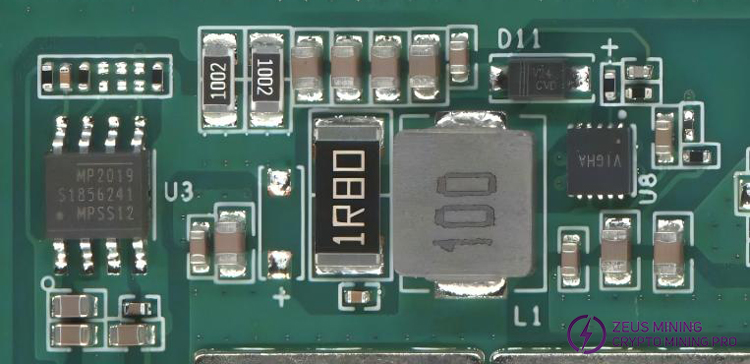
2. H6HB70701 Hash Board Boost Circuit:
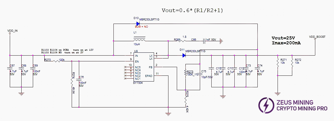
Boost: VDD_IN from the PSU is converted to 25V by U8.
3. H6HB70701 Chip Signal Flow:
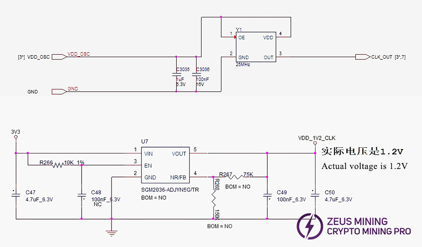
(1) CLK signal flow: Generated by Y1 25MHz crystal. Y1 transmits from chip BM1 to BM95; voltage approx. 0.58-0.6V. Sensor power supplied by U7. If no CLK output, check power first.
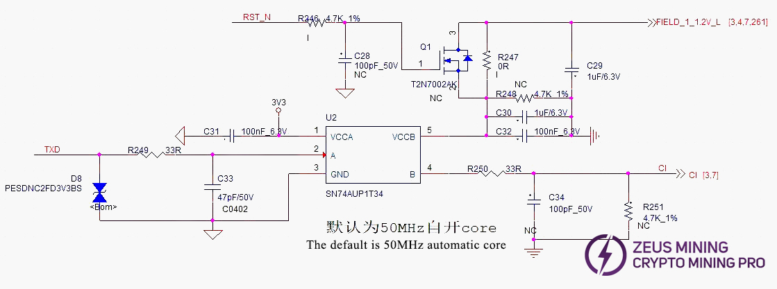
(2) TX (CI, CO) signal flow: Enters from IO port pin 7 (3.3V), passes through level shift IC U2, then transmits from chip BM1 to BM95. Multimeter measures approx. 1.1V.
(3) RX (RI, RO) signal flow: From chip BM95 back to BM1, passes through U1, returns to IO port pin 8, then back to control board. Multimeter measures approx. 1.1V.
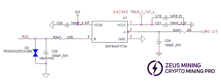
(4) BO (BI, BO) signal flow: From chip BM1 towards BM95.
(5) RST signal flow: Enters from IO port pin 3, passes through R246, then transmits from chip BM1 to BM95. Multimeter measures approx. 1.2V.
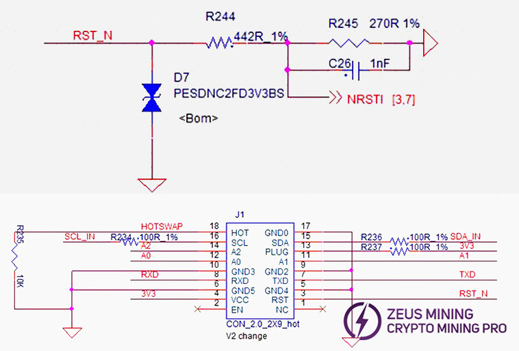
(6) level_shifter 0-17 circuit schematic example (showing one):
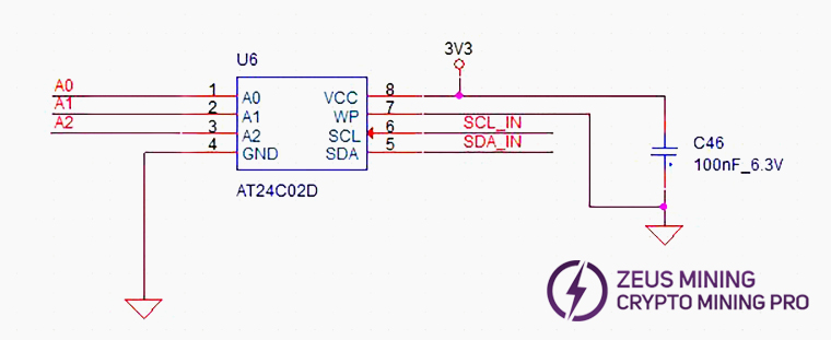
(7) EEPROM schematic:
4. Whole Machine Architecture:
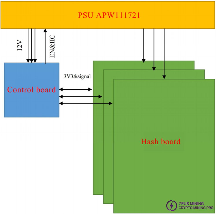
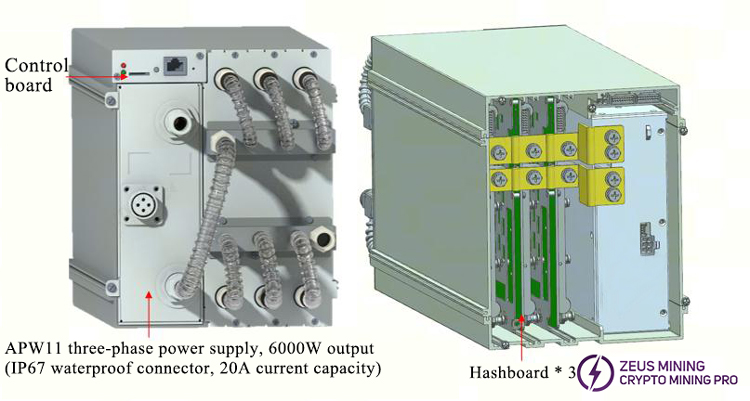
The whole miner mainly consists of 3 hash boards, 1 control board, and one APW111721X power supply.
V. Common Hash Board Failure Phenomena and Troubleshooting Steps
1. Phenomenon: Single board test detects 0 chips (PT1/PT3)
Step 1: First troubleshoot power supply output.
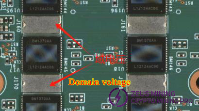
Step 2: Check domain voltage output (CAUTION: Measure on BOT side WITH heatsink secured. Without heatsink will cause burnout).
Measure whether the domain voltage of about 1.1V is normal. If VDD_IN is powered, there is usually domain voltage. Measure the output of the power terminal of the hash board first.
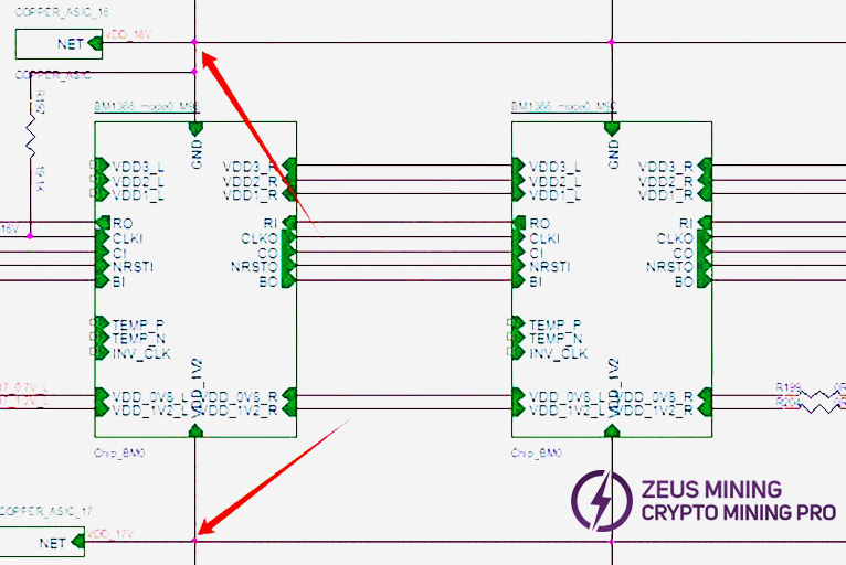
Step 3: Check if CLK is output. Measure before and after BM1. If output is present, measure the last chip (BM95) for CLK. If not, use the 2-point method for maintenance.

Step 4: Check each group's LDO 1.2V, 0.7V output for normal.
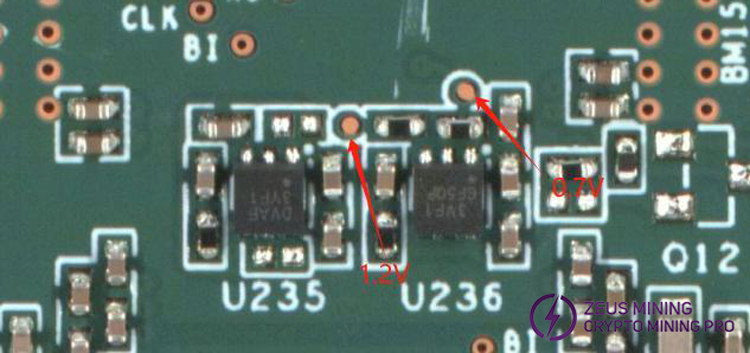
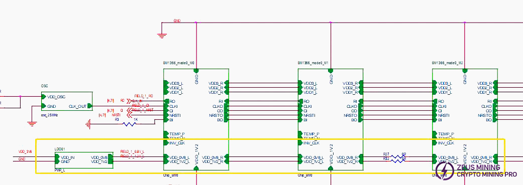
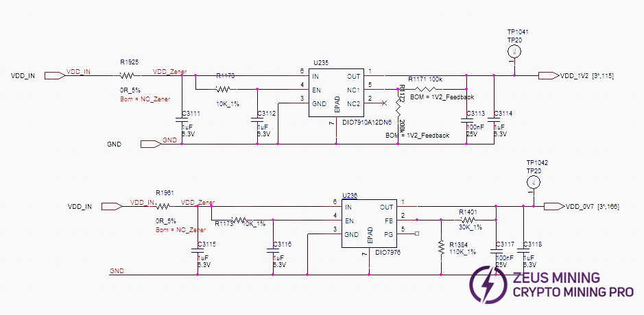
Step 5: Check chip signal outputs (CLK/CI/RI/BO/RST).
Refer to voltage ranges described in the signal flow section. If measured voltage deviates significantly, compare with adjacent group measurements.
Step 6: If voltages and CLK are OK, use the 2-point method. Short the RO test point and 1V2 test point between the first and second chips, then run the chip detection program. Observe the serial log. If still 0 chips found, it will be one of the following:
(1) Use a multimeter to measure the 1V2, 0V7 test points. If not, it may be that the 1.2V, 0.7VLDO circuit of the domain is abnormal, or the two ASIC chips of this domain are not soldered properly. Most of the time, it is caused by a short circuit of the 0.7V, 1.2v chip filter capacitors (measure the resistance of the chip filter capacitors related to the front and back of the PCBA), or measure whether the ground value of the chip VDDIO is abnormal. If it is abnormal, disconnect one of the chips in the domain and find a chip with lower internal resistance to replace it.
(2) Check U1 and U2 circuits for abnormalities, like resistor cold joints.
(3) If 1V2, 0V7 are normal, sequentially measure RO, RST, CLK, CI, BI signals for normalcy.
(4) Abnormal water temperature or heat dissipation can cause U4, U5 burnout, resulting in no 1.2V and 0.7V output for the first domain, and BM1, BM2 chip burnout (U4, U5 burned).
a) If one chip can be found after the binary search short circuit, it means that the first chip and the previous circuits are good. Use a similar method to check the subsequent chips.
E.g., short the 1V2 and RO test points between chip 38 and 39. If the log finds 38 chips, the first 38 chips are fine. If still 0 chips, first check if that 1V2 is normal. If normal, the problem lies with chips after 38. Continue binary search until finding the faulty chip.
Suppose chip N is faulty. When shorting between chip N-1 and N, N-1 chips are found. But when shorting between chip N and N+1, not all chips are found.
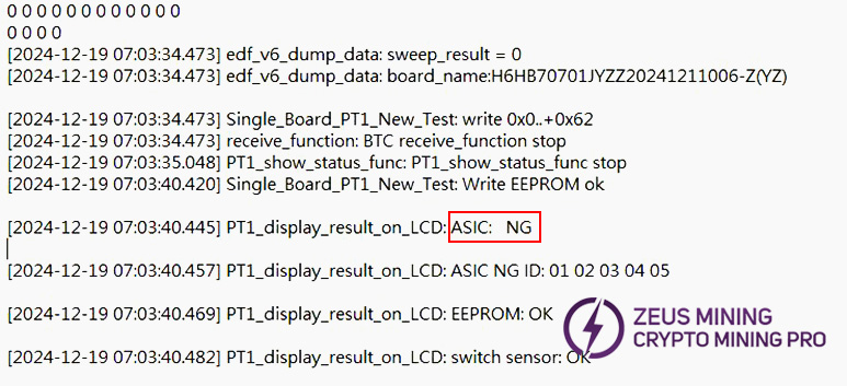
b) LCD displays ASIC NG: (X) (fixed reporting a specific chip), divided into two cases:
d-1) First case: Test time is almost the same as an OK board (usually X doesn't change between tests) (Test time = time from pressing start to LCD showing ASIC NG: (X)). This is likely caused by abnormal soldering of the CLK, CI, BO series resistors around chip X. Focus on checking these 6 resistors. Small probability caused by poor soldering of specific pins on chips X-1, X, or X+1.
d-2) Second case: Chip appearance normal, voltage and signals normal - likely the chip itself is faulty.
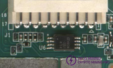
2. Fixture LCD displays EEPROM NG: Check U6 soldering.
3. Fixture LCD displays sensor NG: Test reads temperature abnormally. Troubleshoot as follows:
A) Check serial log. If sensor=0, check U4, U5 chips or nearby SMD resistor and capacitor soldering.
B) Sensor={0, 1}; Corresponding sensor positions {U4, U5}. Prioritize checking if 3.3V power is normal (output from control board to J1). Simultaneously check U98, cold joints can also cause temperature anomalies.
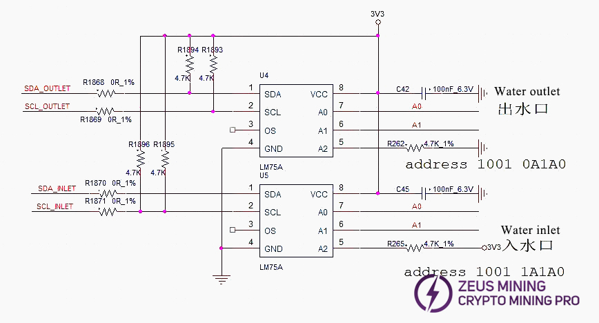
4. Fixture LCD displays INIT NG WATER_TEMP: Test reads inlet or outlet water temperature abnormally. Check U4, U5 and SMD resistor or capacitor soldering.
5. Phenomenon: Multiple chips bad, i.e., nonce rate slightly low (PT3 station)
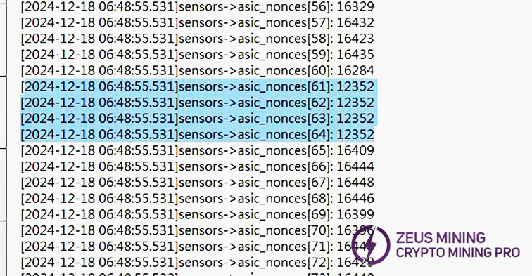
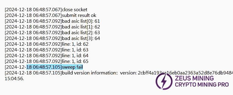
1) First, troubleshoot water flow. Confirm test flow rate is within requirements. H6HB70701 water temp and flow directly affects test results.
2) If flow normal, confirm copper bar voltage is within standard range, check for voltage drop between fixture PSU output and hash board terminal.
3) After eliminating process-related factors, troubleshoot heat dissipation (liquid cooling plate). If there are no abnormalities, replace the chips within 3 chips for repair.
6. Phenomenon: Bad ASIC - entire domain or multiple domains (caused by abnormal domain voltage during trial production)
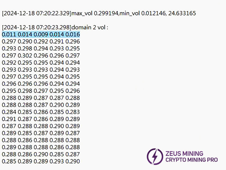
1) Retest the single board and capture test log. If the first domain voltage is found significantly low (as in the example log image), troubleshoot and repair the first domain voltage accordingly.
7. Phenomenon: 1 or a few chips Pattern NG, i.e., incomplete nonce reply data (PT3 station)
1) Check single chip heat dissipation for abnormalities. Visually inspect chip surface for foreign objects, die damage. Usually requires replacing that chip.
2) Chip solder bridging, chip cold joint (a domain with two chips reporting nonce count 0 or 1).
3) Domain voltage slightly low, 1.2V & 0.7V normal - likely bad chip.
4) Multiple chips or entire domain nonce reply abnormal - measure domain voltages, troubleshoot starting from the domain with low voltage.
PS: Crucial: Domain and ASIC numbering start from 0. Residual flux on chip surface (which solidifies and creates gaps with the heatsink) can also cause incomplete nonce replies (MUST clean residual flux thoroughly after chip replacement repair).
VI. Whole Machine Common Failure Phenomena and Repair
1. Whole Machine Initial Test
Refer to test process documents. Issues are usually assembly and process problems or control board process issues.
Common phenomena: Cannot detect IP, Chain detection abnormal. If an exception occurs during testing, repair based on the monitoring interface and test LOG prompts. Whole machine initial test mainly locates faulty control board, PSU, or hash board for swapping and repair.
1) Phenomenon: P:1 (Prioritize checking inlet water temperature for over-temperature, water flow rate. Usually caused by temperature exceeding standard triggering OTP. If a specific chip OTP is indicated, after checking water temp and flow, check if hash board heat dissipation is abnormal).
2) Phenomenon: JX:1 (Chip bad ASIC. Prioritize heat dissipation. If heat dissipation normal, usually bad chip).
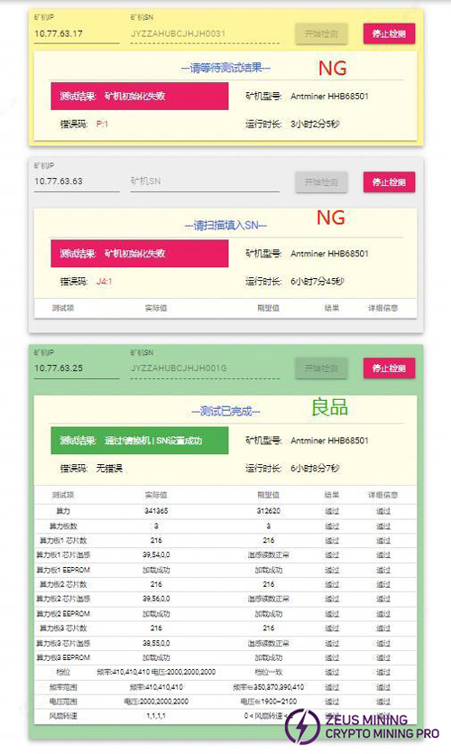
2. Aging test: During the aging test, maintenance should be carried out according to the monitored interface test. E.g.:
1) Missing chain: Missing chain means one of the three boards is missing. Mostly due to connection issues between hash board and control board. Check cables for open circuits. If connection OK, perform PT3 test on the single board. If it passes, likely a control board issue. If fails, repair using PT3 methods.
2) Temperature Abnormal: Usually high temperature. Monitoring system limits: PCB temp ≤80°C, Chip temp ≤95°C. Exceeding causes alarm and shutdown. Check if outlet water temp exceeds 45°C. Also, thermal gel issues can cause temperature anomalies.
3) Cannot Find All Chips (OM firmware can boot and run, IM firmware cannot run. OM firmware hashrate is 2/3 or 1/3 of normal). Check log for insufficient chip count. If chip count insufficient, refer to PT1&PT3 test repair.
4) No Hashrate After Running a While, Pool Connection Lost: Check network.
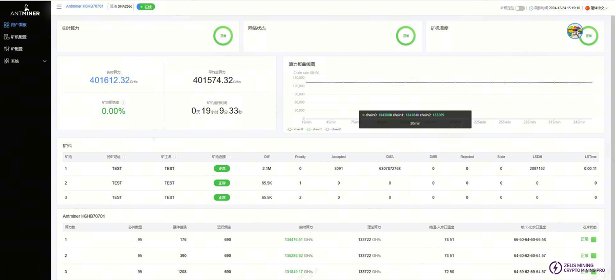
5) Aging test status of normal good quality machine
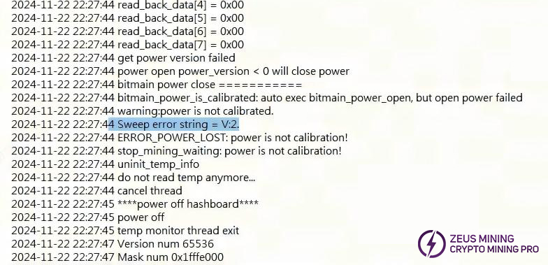
3. Whole Machine Test V:2 Failure
Prioritize checking whether the voltage regulator cable is assembled OK. Generally, if the voltage regulator cable is not assembled properly or is loose, it will cause V:2 failure. Then perform cross power supply verification.
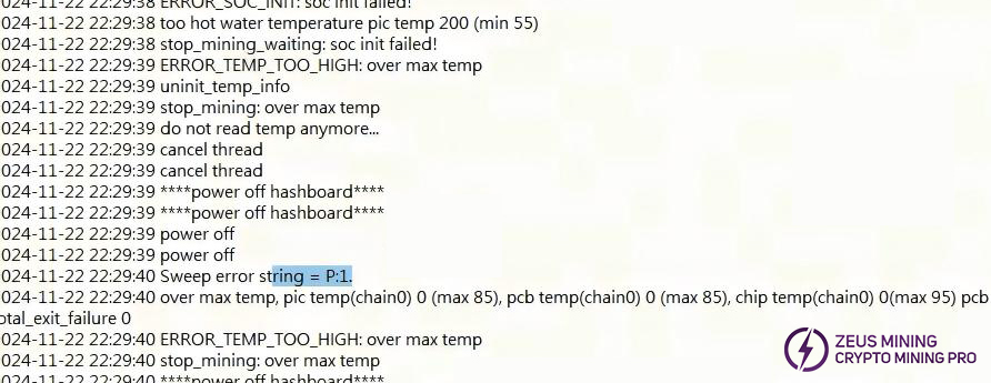
4. Whole Machine Test P:1 Failure
Retest to confirm aging rack water flow and temp is normal. Then check log for over-temperature location and repair accordingly.
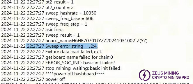
5. Whole Machine Test JX:4 Failure
Remove the corresponding faulty board for retest and frequency sweep, generally it will test NG and repair it according to the bad board. Assembly collision and other bad.
6. Whole Machine Test JX:1
Single or multiple chips marked X. Prioritize heat dissipation. Pilot production also found issues caused by solder bridging under chips. After process checks, replace the corresponding chip(s).
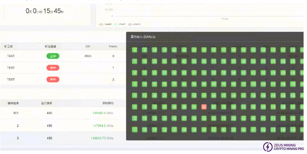
7. Whole Machine Does Not Boot
Repair according to log prompts. Usually perform cross verification to determine if hash board, PSU, or control board is faulty, then target repair. Log example shown usually indicates cable issue or component damage near J1. Find the corresponding chain to troubleshoot. If all normal, EEPROM info might be lost; retest PT.
VII. Control Board Problems Leading to the Following Issues
1. Whole machine does not run
1) Check if voltage outputs at key points are normal. If 3.3V shorted, first disconnect U8. If still shorted, remove CPU and measure. For other voltage abnormalities, usually replace the corresponding voltage regulator IC.
2) If voltages normal, check DDR and CPU soldering (Production end X-RAY check).
3) Try using SD card to update flash program.
If the miner that has been flashed with the control board card needs to start normally, the following operations are required:
a) After successful card flash, green LED solid on. Power off and restart.
b) After repowering, wait 30s (OTP opening process).
c) OTP (One Time Programmable) is a type of MCU memory. Program burned into IC cannot be changed or erased again.
Precautions:
① Sudden power loss during OTP opening or waiting less than 30s will cause control board OTP function failure, preventing startup (no networking). Requires replacing U1 (control board main IC FBGA). The replaced U1 cannot be used on 19 series boards again.
② Control boards that have had OTP opened cannot have their U1 used on other series models.

2. Whole machine cannot find IP
Mostly caused by abnormal operation (Refer to point 1 troubleshooting).
Check Ethernet port, network transformer T1, CPU appearance, and soldering.
3. Whole machine cannot upgrade
Check Ethernet port, network transformer T1, CPU appearance, and soldering.
4. Whole machine reads hash board failure or missing chain, reports J :1
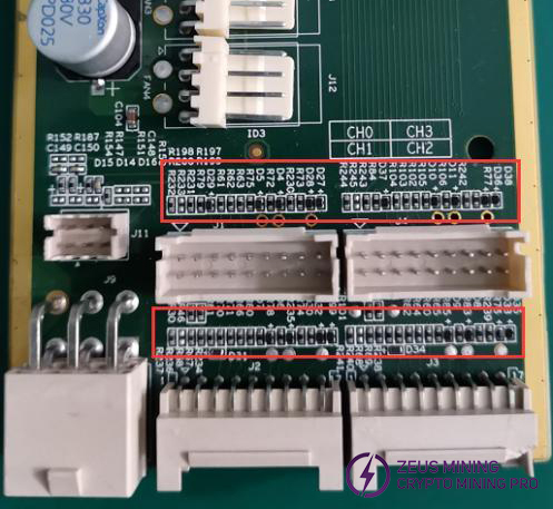
A. Check cable connection status.
B. Check components on the control board for the corresponding chain.
C. Check wave soldering quality of cable header pins and resistors around the connector interface.
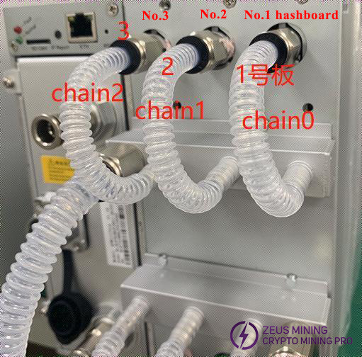
Log prompt "find x asic" (x < 95) indicates incomplete chip detection on that hash board. Repair as PT1 chip detection failure. [Chain0] represents board 1, [Chain2] represents hash board 3 (next to PSU). Middle board is [Chain1] (board 2).
Note: If all 3 boards show incomplete chips, troubleshoot PSU, voltage adjustment cable, control board.
5. After-sales repair, production maintenance water cooling test platform setup (Test water temp: 32-35℃, Single board water flow rate 2-3L/min)
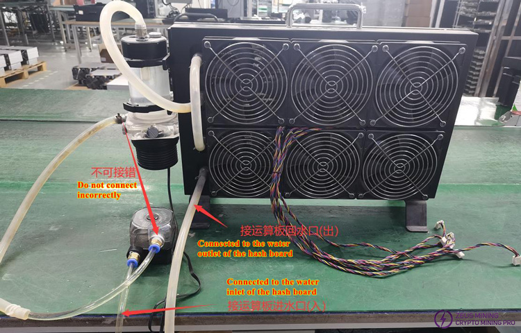

1) Since the first-gen water block cannot meet requirements, when modifying, add a water pump in series (or connect 2 water blocks in series), or test on the production test bench. Alternatively, purchase a better performing water block as shown below. Production end recommended to use the test water-cooling bench. Regular water blocks can be used for PT1 repair testing.
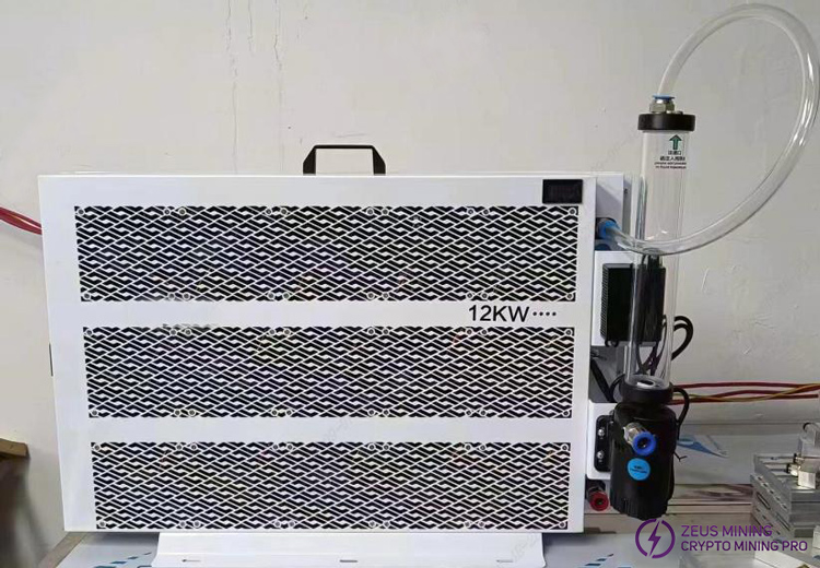
2) Use 8mm water pipe fittings during modification. If heat dissipation insufficient, add auxiliary air cooling fans.
After repair, test PT1 using barcode scan mode before testing PT3.
VIII. Other Precautions
Repair Flow Chart

1. Routine Inspection:
First, visually inspect the hash board for PCB deformation, burn marks. Address these first if found.
Check for obviously burned components, impact damage, misalignment, or missing parts.
If visual OK, measure impedance of each voltage domain to check for shorts or opens. Address any found.
Then, check if each domain voltage is around 1.2V.
2. After routine inspection (short check is mandatory to prevent burnout upon power-up), use test fixture for chip detection. Troubleshoot based on fixture results.
3. According to the display results of the test fixture detection, start from the vicinity of the faulty chip and detect the chip test points (CI/RST/RO/CLK/BI) and voltages such as VDD0V7 and VDD1V2.
4. Then according to the signal flow, except for the RO signal which is transmitted in the reverse direction (chip No. 95 to chip No. 1), several signals CLK CI BI RST are transmitted in the forward direction (1-95), and the abnormal fault point is found through the power supply sequence.
5. When locating the faulty chip, the chip needs to be re-soldered. The method is to add flux around the chip (preferably no-clean flux), heat the solder joints of the chip pins until they are dissolved, and promote the chip pins to re-grind with the pads and collect the tin. This will achieve the effect of re-tinning. If the fault is still the same after re-soldering, the chip can be directly replaced.
6. After the repair, the hash board must pass the test twice to be considered as a good product. The first time, after the replacement of the parts, wait for the hash board to cool down, use the test fixture to test it, and then put it aside to cool down. The second time, wait a few minutes until the hash board is completely cooled, and then test it again.
7. After the hash board is repaired, relevant maintenance and analysis records must be made (repair report requirements: date, SN, PCB version, bit number, defect cause, defect responsibility, etc.). In order to provide feedback to production, after-sales, and R&D.
8. After recording, assemble the whole miner for regular aging.
9. The good products repaired by the production end must be streamlined from the first production station (at least the appearance and PT1/PT3 test stations must be inspected).
10. For the repaired defective hash board, the heat sink thermal gel must be reprinted (otherwise it will cause temperature abnormalities) before it can be streamlined.
Dear Customers,
Hello, May 1-5, 2026 (GMT+8) is China's May Day, and international logistics will be suspended. Our company will suspend shipments on the afternoon of April 30, 2026, and resume warehouse shipments on May 6 (GMT+8). We are deeply sorry for the inconvenience caused to you. Thank you for your trust and support.
Best wishes,
ZEUS MINING CO., LTD.