

P221 Power Supply Series Repair Manual V1.2
Contents
P221 Power Supply Series Product Description
Remove screws from the housing and PCB board of the P221 power supply series.
P221 power supply series schematic diagram
Troubleshooting Guide for P221 Power Supply Series (Visual Inspection & Multimeter Measurement)
P221 Power Supply Series: Replacement of Faulty Components
P221 Power Supply Series Function Test Judgment Method
P221 Power Supply Series Assembly
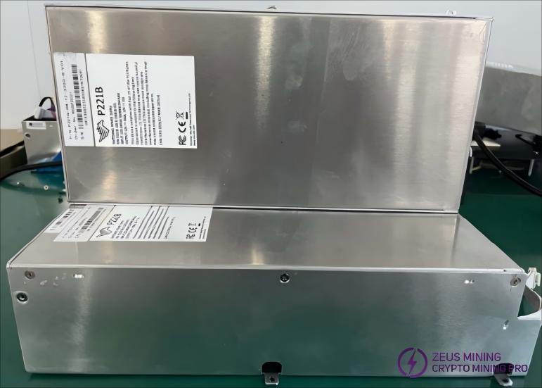
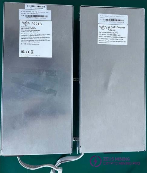
1.P221C/B Power Supply Series Product Description
Power supply specifications: (G1355/3600W, output voltage adjustable via IIC)
2. Remove screws from the casing and PCB board in the P221C/B power supply series
2.1 First, check if the power supply is working correctly (you can power it on separately to confirm)
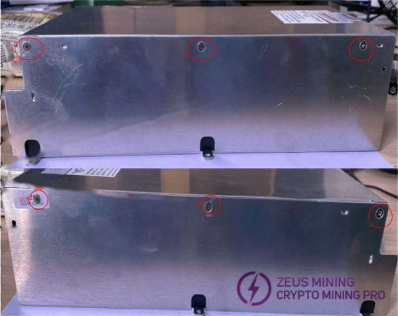
2.2 Power supply housing disassembly:
Remove the shell fixing screws (6 in total)
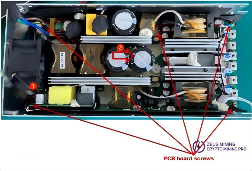
2.3 Power supply disassembly:
Before separating the PCB board, first disconnect the fan socket cable as shown in Figure 1.
After unscrewing the five screws, remove the PCB board to the right, as shown in Figure 2.
2.4 PCB board classification:
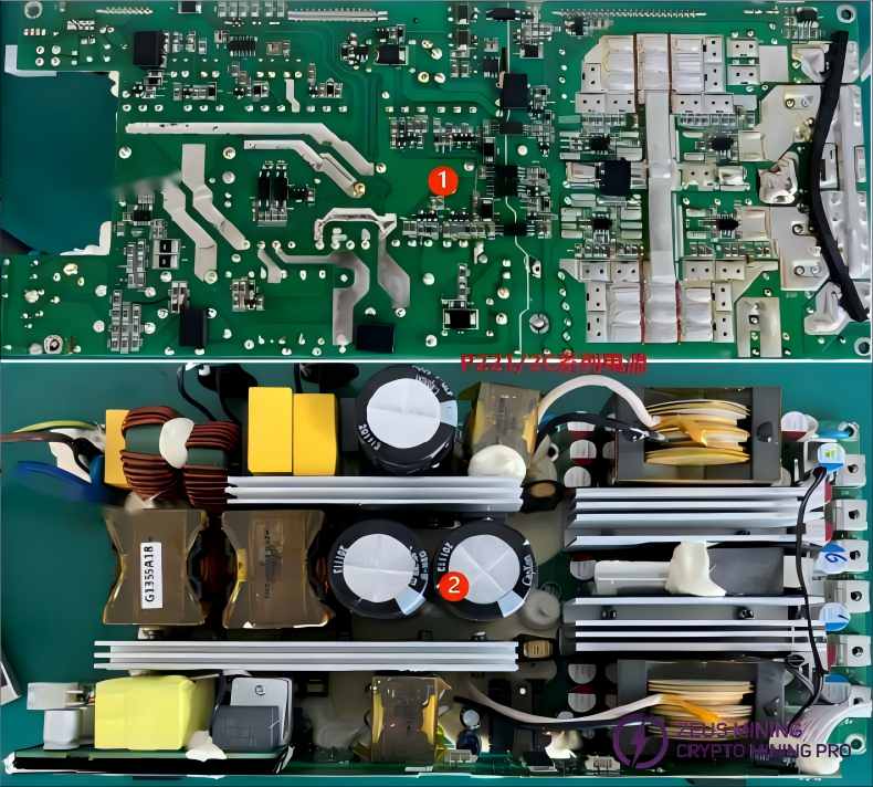
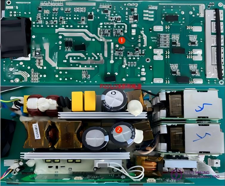
As shown in Figure 1, the PCB SMT component surface/solder surface
PCB component side, as shown in Figure 2
P221/2C Series Power Supplies:
P221/2B Series Power Supplies:
3. P221C/B Power Supply Series Schematic Diagram
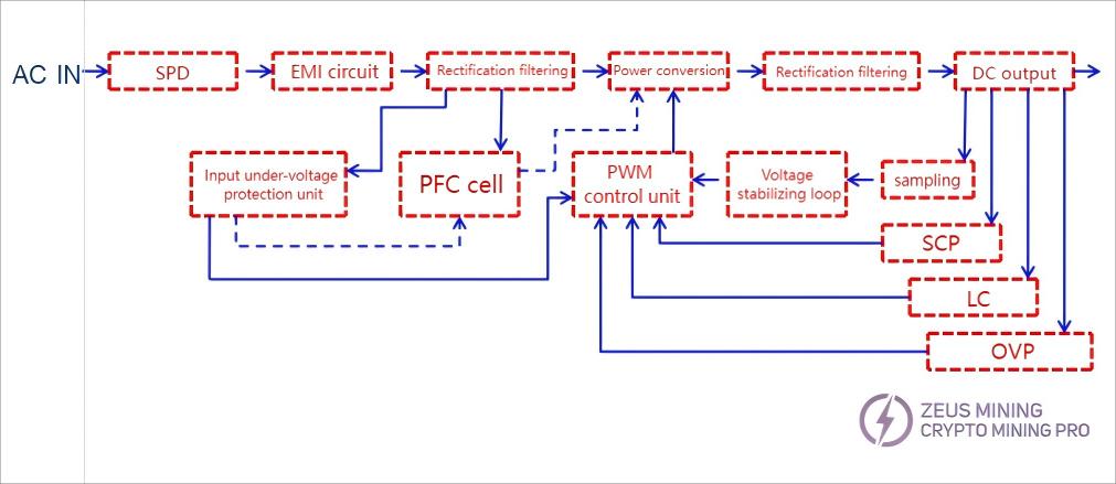
3.1 Switching power supply block diagram:
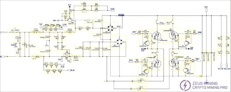
3.2 Schematic Diagram of P221 Series Power Supply Circuit:

3.3 Summary of Faults Returned to P221 Power Supply Series:
order number | unhealthy phenomenon | Bad reason | Part number | point location |
1 | no-output | PFC fault | F1,MOS transistor, main control chip | F1 Q86 Q6 Q21 Q84 Q22 Q41 D20 D2 U13、U14 |
2 | communication failure | The MCU board is damaged due to harsh environmental conditions, and the communication cables are damaged. | Communication cables, MCU chips | J28 U37 |
3 | The power supply is powered on normally and has no output. | MOS damaged due to overload operation | synchronous rectification MOS | Q4 Q5 Q6 Q15 Q16 Q21 Q22 Q23 Q24 Q25 Q26 Q29 |
4 | The output cable terminal is faulty | The output cable terminal is damaged or the output cable has poor contact. | Output cables and terminals | J28 |
5 | Destroyer | The internal high-voltage component in the power supply is prone to dust accumulation, which may reduce the safety clearance of MOSFETs and potentially cause device failure. | F1, MOSFET, main control chip, PCBA | F1 1 Q86 Q6 Q21 Q84 Q22 Q41 D20 D2 U13 U14 R61 R30 R15 R54 |
6 | report fault code | Insufficient output power (e.g., recalibration required after replacing the downstream MCU chip) | AATE testing software | recalibration |
4.P221 Power Supply Series Fault Repair Method
4.1 P221/2C Power Supply Troubleshooting Method (Visual Inspection)
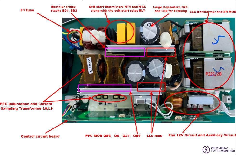
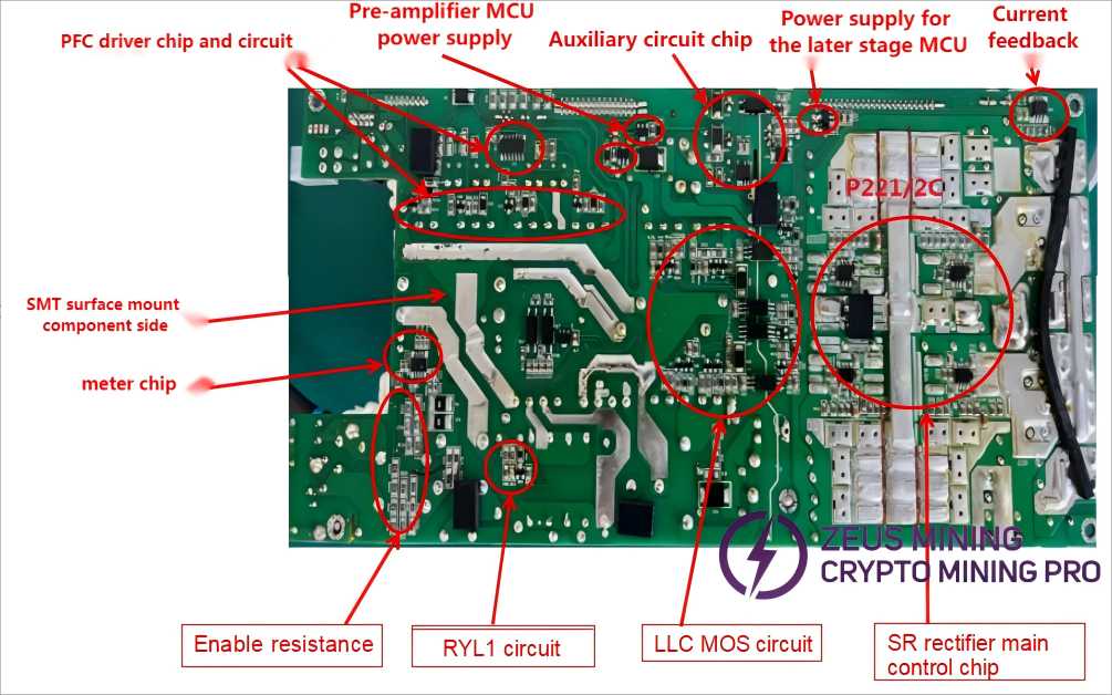
PCB Visual Inspection: First, visually inspect the surface of electronic components (such as MOS transistors, fuses, large capacitors, transformers, etc.) and check the following locations for noticeable burn marks or spark marks between the components and the heat sink: RLY1, NT1/NT2, BD1/BD3, Q86/Q22, Q21/Q23, F1, C23/C68, etc., as shown in the figure.
Next, visually inspect the SMT and solder surfaces for any burnt electronic components or copper-plating spark marks, as shown in the figure.
4.2 P221/2B Power Supply Troubleshooting Method (Visual Inspection)
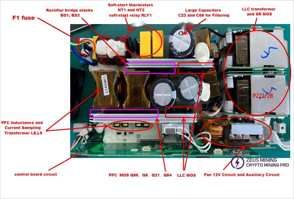
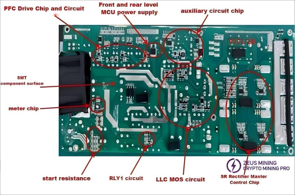
First, visually inspect the electronic components (MOSFETs, fuses, large capacitors, transformers, etc.) to check for obvious signs of burning or arcing between the components and the heat sink, such as RLY1, NT1/NT2, BD1/BD3, Q86/Q22, Q21/Q23, F1, C23/C68, etc., as shown in the figure.
Next, visually inspect the SMT/surface-mount component side/solder side for any burnt electronic components or signs of arcing between components and copper traces, as shown in the diagram.
4.3 PCB visual inspection method
Next, visually inspect the DIP component side/solder side for any burnt electronic components or signs of arcing between components and copper traces, as shown in the diagram.
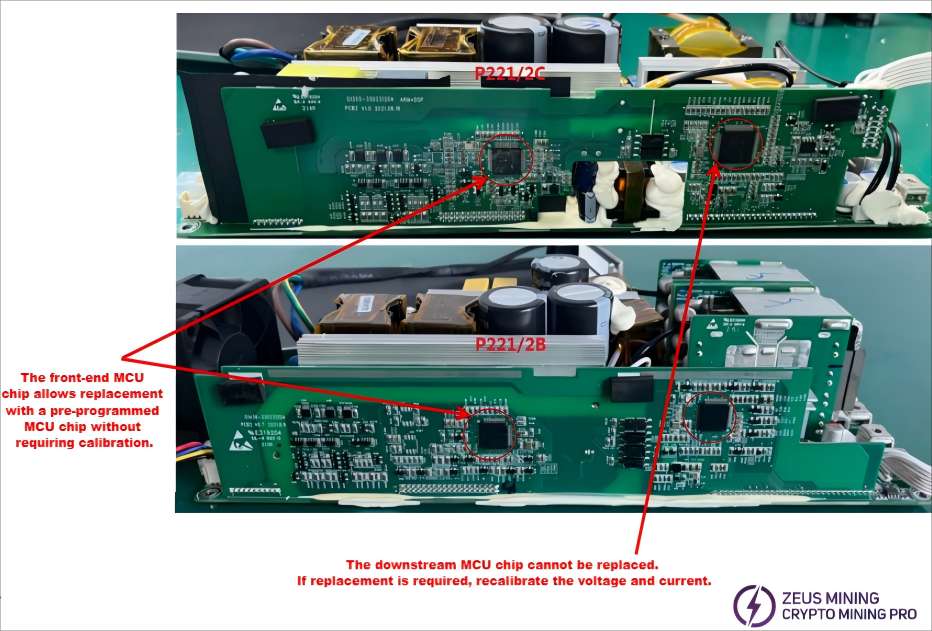
Note: The calibration parameters of the downstream MCU chip are embedded in the chip and cannot be replaced during maintenance, as doing so would erase them.
4.4 PCB Multimeter Testing Method:
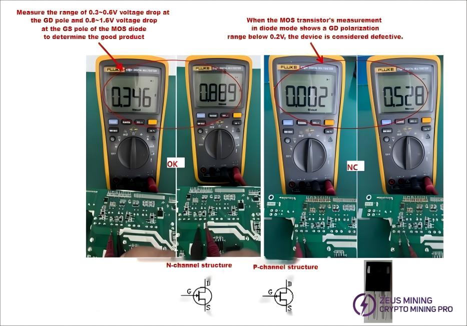
MOSFETs, rectifier bridges, and ordinary transistors are tested using a multimeter's diode test mode. A voltage drop of 0.3-0.6V between two pins indicates a good component; otherwise, it is considered a breakdown failure, as shown in the diagram:
4.4.1 PCB Multimeter Testing Method:
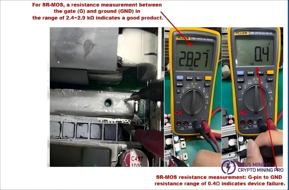
Resistance measurement method: Connect the black probe to ground and use the red probe to measure the resistance between the gate (G) terminal of the SR tube and GND. The lowest resistance reading, especially if it is below 1.5 kΩ, indicates a device failure, as shown in the diagram on the right.
4.4.2 PCB Multimeter Inspection Method:
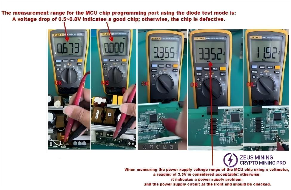
MCU Chip Programming
Measure the voltage drop using the diode test mode:
A voltage drop of 0.5~0.8V indicates the chip is functioning correctly; otherwise, the chip is faulty. Measure the power supply voltage using voltage mode: 3.3V is standard; otherwise, the power supply is defective, as shown in the figure below.
4.4.3 PCB Multimeter Testing Method:
First, check whether the working voltage of each group is within the normal range. The auxiliary power supply circuit must be functioning properly; other circuits can only function when the VCC voltage is within specification. The power supply section operates at high voltage, so please be extremely careful during operation. Non-professionals should not disassemble the equipment! The voltage values of each circuit are shown in the figure below:
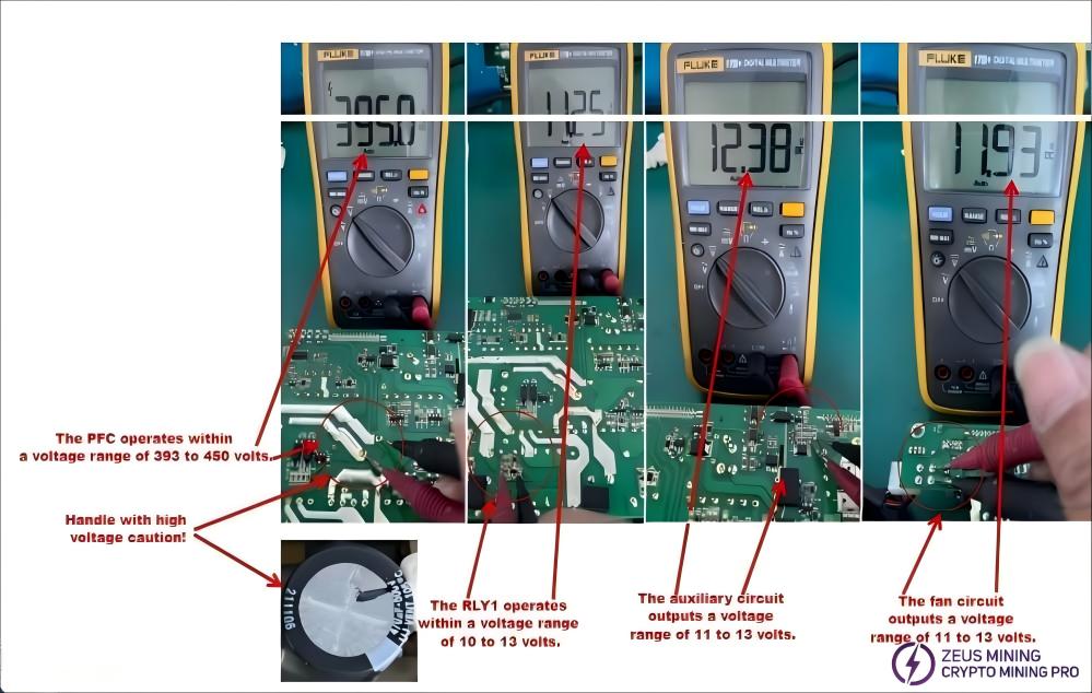
4.4.4 PCB Multimeter Testing Method:
First, check whether the working voltage for each group is within normal limits. The auxiliary power supply circuit must be operating on VCC before other circuits will operate. The power supply unit operates at a high voltage; operate with caution. Non-professionals should not disassemble the device! The voltages of each circuit are shown in the diagram:
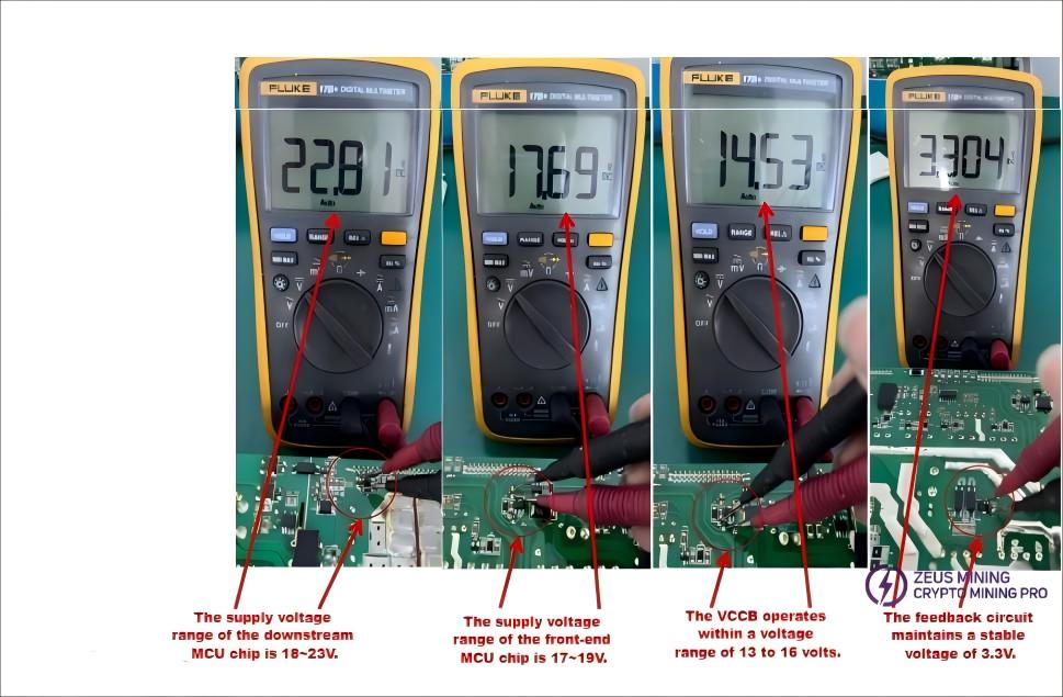
4.4.5 PCB Multimeter Testing Method:
First, check whether each circuit's operating voltage is within the normal range. The auxiliary power supply circuit must be working correctly and providing the VCC voltage for other circuits to operate. The power supply unit operates at high voltage, so exercise caution during operation. Non-professionals should not disassemble the equipment! The voltage values for each circuit are shown in the figure below:
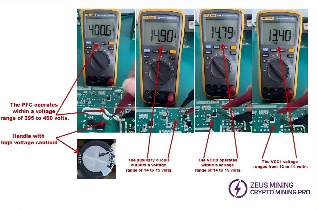
4.5 PCB Multimeter Testing Method:
First, check if the working voltage of each group is within the normal range. The auxiliary power supply circuit must be functioning properly; other circuits can only operate once the VCC voltage is standard. The power supply contains high voltage; please be extremely careful during operation. Non-professionals should not disassemble it!
Note:
(1) Please refer to Section 3.1 for the circuit diagram of the P221C series power supply.
(2) The testing and repair methods for the P221C series power supply are the same as those for the P221B power supply; please refer to Section 4.4 PCB Multimeter Testing Method.
(3) The secondary main control chip of the P221 series power supply cannot be replaced arbitrarily, as this chip contains power supply current and voltage calibration parameters. The main control chip only supports firmware upgrades. If the secondary main control chip needs to be replaced, power supply current and voltage calibration tests must be performed to ensure it meets factory standards.
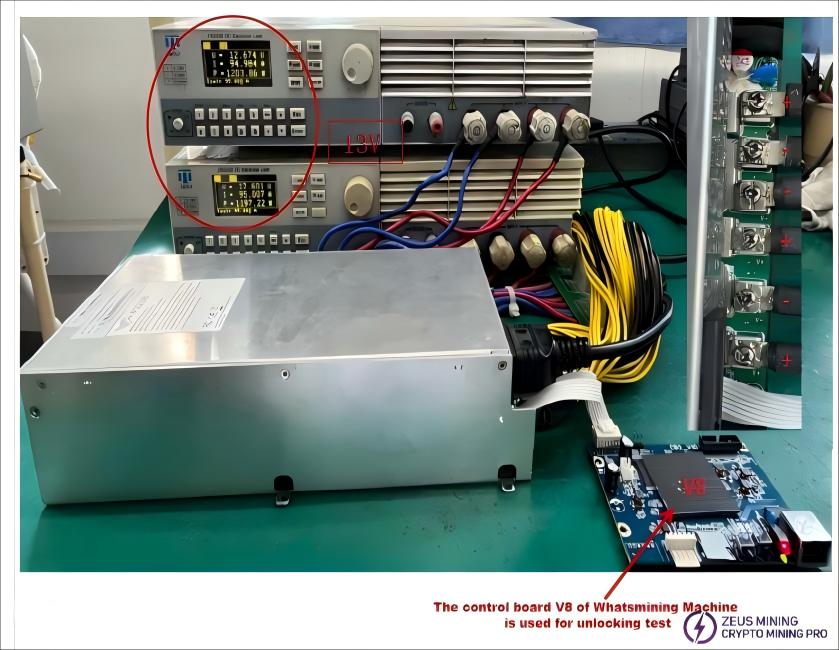
(4) After the power supply repair is completed, please use an electronic load for a 15-minute full-load test to confirm that the power supply is working normally (you can also use a mining machine for aging testing).
(5)The Shenma Miner V8 control board (with a dedicated power supply unlocking program) can be used to unlock the power supply for load testing.
(6)The P221C/B and P222C/B power supplies have basically the same structure, with only slight differences in output voltage and power (P221C/B is 12V, P222C/B is 14.5V). For detailed information, please refer to the technical specifications on the product nameplate.
Equipment list required for P221 power supply series maintenance:
order number | Equipment model | Equipment specifications | quantity | Remark |
1 | electronic load | 3 unit | Product output, load voltage, and current calibration | |
2 | AC short-circuit circuit | 1 unit | It protects against short circuits in the high-voltage section of the product. | |
3 | multimeter | 1 unit | Measure and assess the component's status. | |
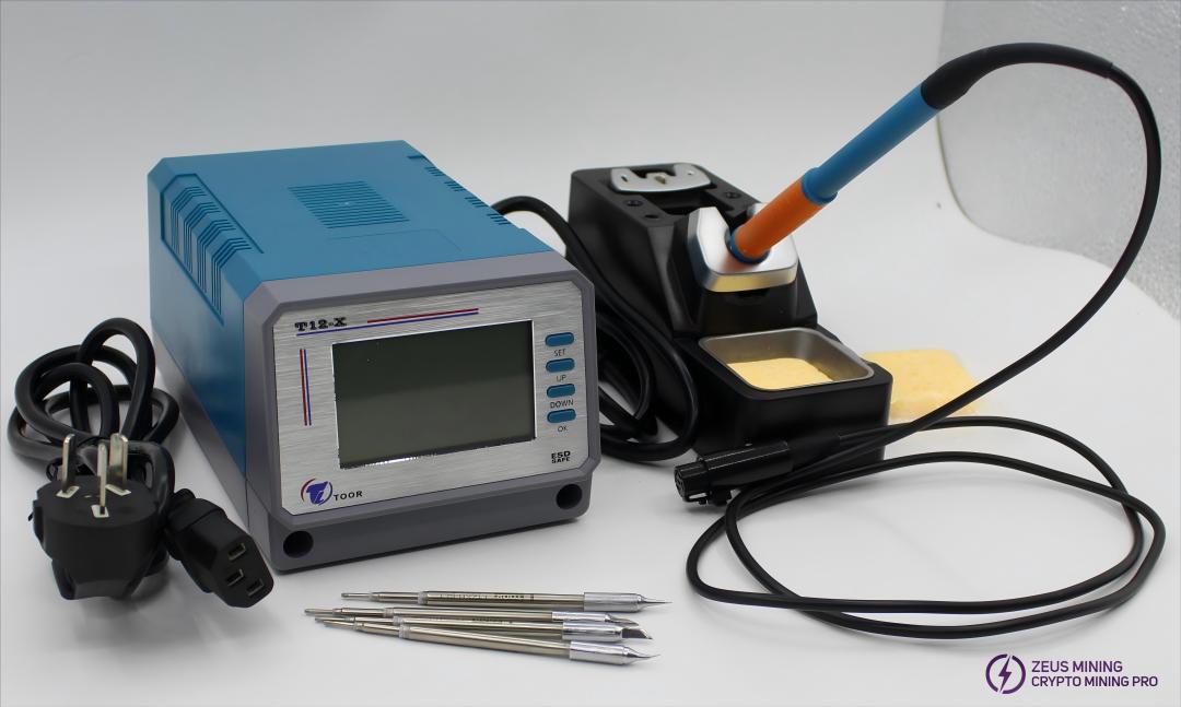
4 | soldering station | 1 unit | Intelligent temperature control technology | |
5 | Desoldering station | 1 unit | Remove the defective components. | |
6 | tool | 3 unit | Needle-nose pliers, Diagonal pliers, screwdriver |
Note: The above equipment can be purchased from Zeus Mining.
5. Operation of Replacing Bad Components in P221C/B Power Supply Series
5.1 Tool Usage Instructions:
Solder sucker, screwdriver, diagonal pliers, multimeter
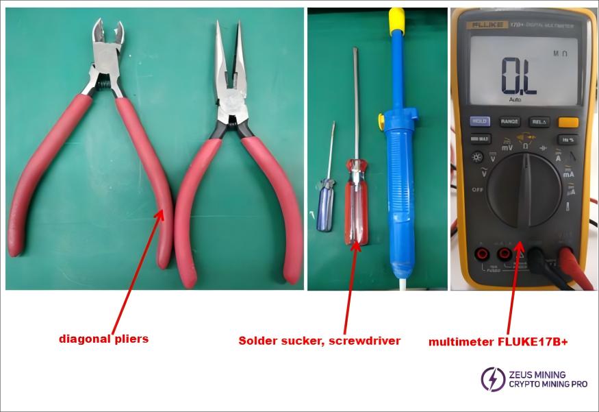
5.2 Tool Usage Instructions:
Constant Temperature Soldering Iron:
1) Replacing MOS transistor components:
High-temperature soldering iron temperature: 400±10℃, soldering time for component pins: 3-4 seconds
2) Replacing surface-mount resistor and capacitor components: Constant temperature soldering iron temperature: 380±10℃,
Soldering time for component pins: 2-3 seconds
5.3 Replacing a faulty MOS transistor:
1) Identify the faulty MOS transistor and use a screwdriver to remove the silicone sealant from it.
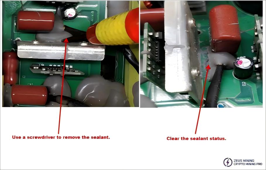
2) Identify the faulty MOS transistor and remove it using a desoldering tool.

3) Remove the MOS transistor by loosening the fixing screws with a screwdriver, then the MOS transistor body can be removed.
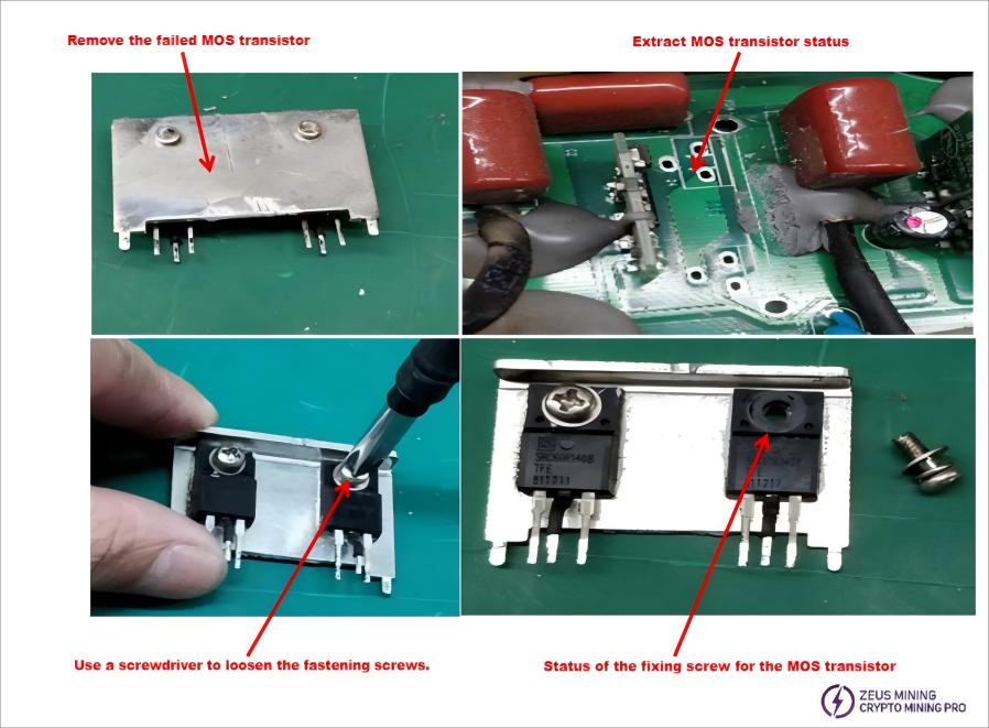
4) Assemble the good quality MOS transistors and solder them; there should be no cold solder joints.

Note: The replacement of other electronic components should also be carried out using the above method.
6. Test and Judgment Method of P221C/B Power Supply Series
Connection diagram for connecting the P221 power supply series output to the electronic load: ● Set the load to CC mode (CC1A) ● Connect the positive (+) and negative (-) terminals of the P221 power supply series output to the corresponding positive (+) and negative (-) terminals of the load's power output. Do not reverse the polarity!
Note: If the customer does not have an electronic load meter, they can also use a mining machine as a load for power-on confirmation.
7. P221C/B Power Supply Series Assembly
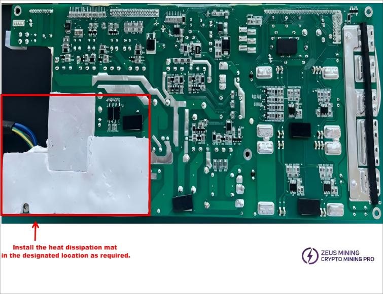
7.1 After repairing faulty power supplies using the above methods, first check if the heat dissipation pads on the PCB have come loose. Refer to the diagram on the right for inspection and reapply them in the correct positions to prevent overheating and protect the power supply during operation.
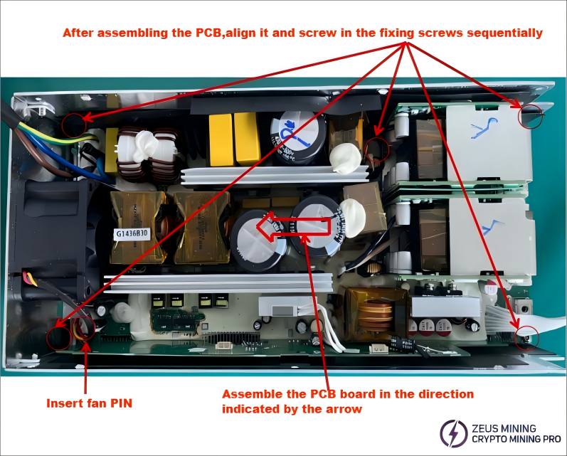
7.2 According to the direction markings on the diagram, install the PCB board into the casing and tighten the corresponding fixing screws. Ensure that no wires are pinched to avoid damaging the insulation layer, as shown in the figure.
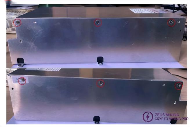
7.3 Full Assembly: After confirming all connections between the upper and lower plates are properly made (as shown on the previous page), install the cover. Align the screw holes of the upper and lower plates, then fasten the outer shell with six screws as illustrated below:
7.4 Complete Assembly: The final assembly of the P221C/B power series unit is shown in the figure below.
