


DG1+ Repair Hash Board Technical Manual
I. Requirements for Repair Platform/Tools/Equipment Preparation:
1. Platform Requirements:
Anti-static workbench (workbench must be grounded), anti-static wrist strap, and grounding.
2. Equipment Requirements:
Constant temperature soldering iron (350°C-380°C); hot air gun, multimeter (pointed probes are recommended for easier measurement); oscilloscope, network cable (requirements: connected to the Internet, stable network).
3. Testing Tool Requirements:
DC power supply (requirements: 15V voltage, 30A current); power adapter cable (self-made: use thick copper wire to connect the power supply and the hash board, 4AWG copper wire within 60cm in length is recommended), used for powering the hash board; 12V DC power supply, used for powering the control board.
4. Repair Auxiliary Materials/Tools Requirements:
Solder paste, flux, PCB cleaning solution and anhydrous alcohol; PCB cleaning solution is used to clean flux residue after repair; thermal conductive gel (specification: Fujipoly SPG-30B) is used to apply to the chip surface after repair; ball grid array stencil, desoldering wick; when replacing a new chip, the chip pins need to be tinned before soldering to the hash board, and thermal conductive gel should be evenly applied to the chip surface before locking the large heat sink.
(1) RS232/TTL adapter board 3.3V
II. Repair Requirements:
1. Pay attention to proper handling techniques when replacing chips. Ensure the PCB shows no significant deformation after replacing components, and check for missing parts, open circuits, or short circuits in the replaced components and surrounding areas.
2. Repair personnel must possess a certain level of electronic knowledge, at least one year of repair experience, and be proficient in BGA/QFN/LGA packaging soldering techniques.
3. After repair, the hash board must be tested at least twice and pass both tests before being considered acceptable.
4. Check that tools and fixtures are working correctly, and confirm the repair station's test software parameters and test fixture versions.
5. For testing after chip replacement, the chip must be tested first. After passing this test, perform a functional test. The functional test must ensure that the small heatsink is properly soldered, the large heatsink is installed correctly (with the thermal paste applied evenly before installation), and the cooling fan is running at full speed. When using a chassis for cooling, two hash boards must be placed simultaneously to create an airflow (essential).
6. When measuring signals, use an auxiliary fan for cooling, keeping the fan at full speed to prevent the hash board temperature from becoming too high and damaging the hash chips.
7. When powering on the hash board, the negative power supply copper wire must be connected first, then the positive power supply copper wire, and finally the signal cable. When disassembling, the order must be reversed: disconnect the signal cable first, then the positive power supply copper wire, and finally the negative power supply copper wire. Failure to follow this order can easily damage the U5 chip (resulting in missing chips). Before testing the pattern, the repaired hash board must cool down; otherwise, it will result in a PNG test.
8. When replacing a new chip, print the pins and solder paste to ensure the chip is pre-tinned before soldering it to the PCBA during repair.
III. Fixture Fabrication and Precautions
The test fixture and accompanying clamps should meet the heat-dissipation requirements of the computing board and facilitate signal measurement.
1. Obtain the test fixture.
2. For the first use of the test fixture, ensure that the control board firmware is the latest version and that the main control board and the computing board are correctly connected.
3. Adjust the DC power supply voltage for the computing board to 20V, and the control board to 12V. For the first power-on, power on the computing board first, then the control board. It is crucial to maintain this sequence; otherwise, the repair software will not function properly.
IV. Overview of the Principle
1. DG1+ Hash Board Working Structure:
The hash board consists of 204 SSL31 chips, divided into 34 groups (domains), with each group consisting of 6 ICs; the working voltage of the SSL31 chips used in the DG1+ hash board is 0.6V; groups 34, 33, and 32 (a total of 3 groups) are powered by 25.8V output from the boost circuit U273, which supplies power to the LDOs (U271, U269, U267), enabling these three domains to output 1.8V and 0.85V. The LDO of group 21 is directly powered by the VDD 18.5V power supply, enabling it to output 1.8V and 0.85V, and the voltage decreases by 0.6V for each subsequent domain.
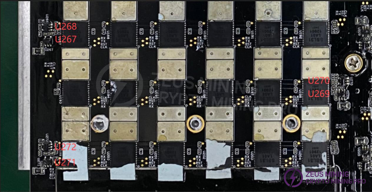
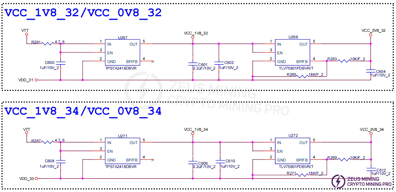
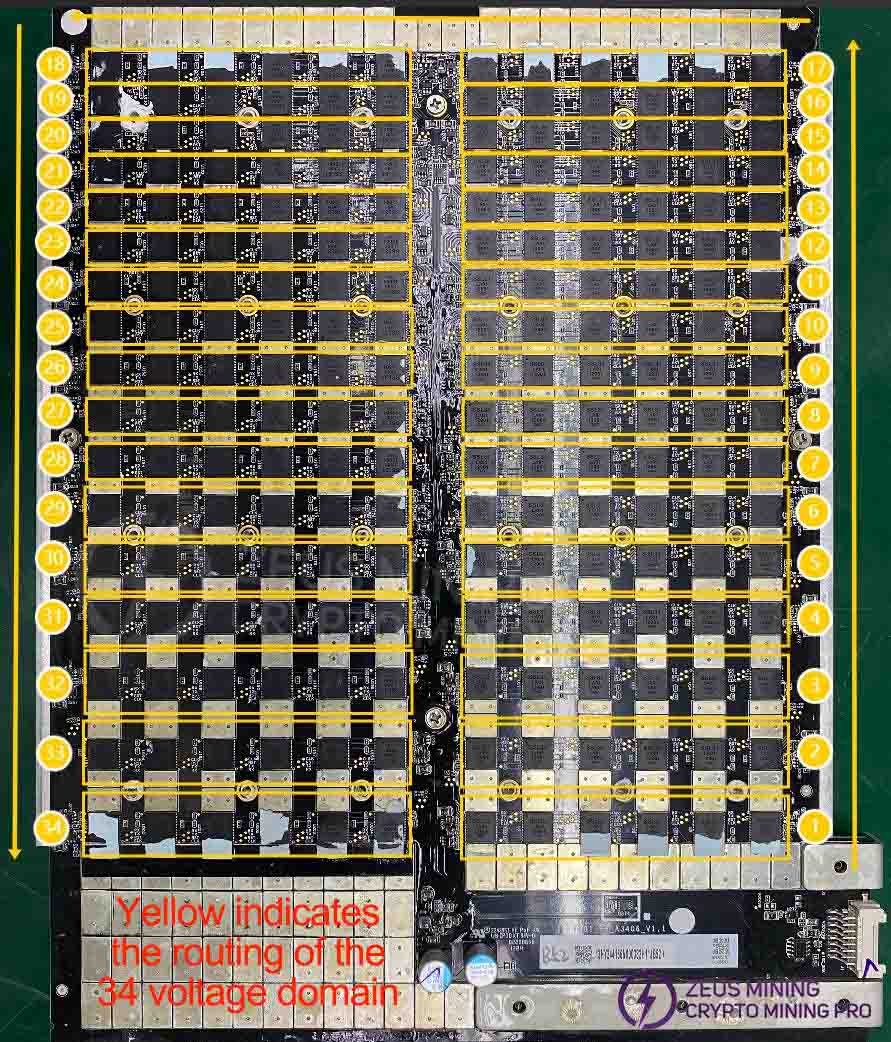
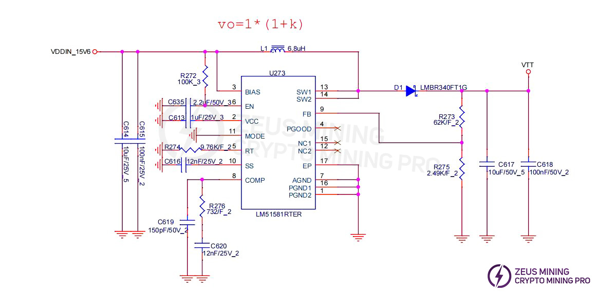
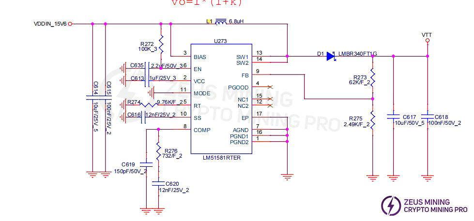
2. DG1+ Computing Board Boost Circuit:The voltage is boosted from 18.5V to 25.8V by the power supply.

3. DG1+ chip signal routing
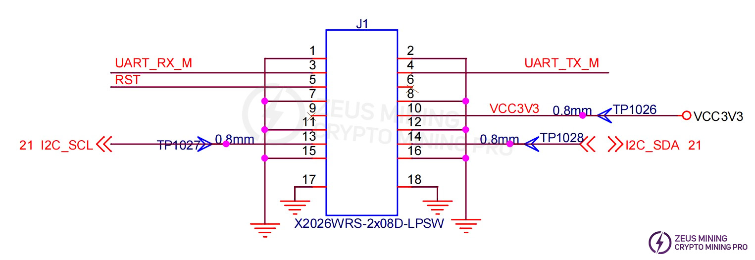
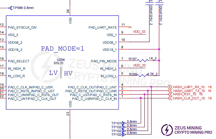
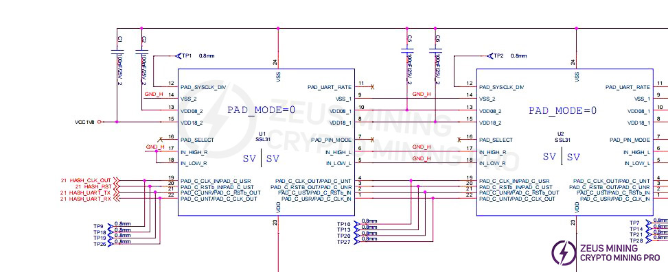
(1) CLK signal flow: A 1.8V (U205 LDO) 15MHz waveform is generated by the X1 active crystal oscillator and provided to all chips from chip #1 to chip #204 through series resistor R277; the clock signal measured by a multimeter from chip ID 0 to chip ID 203 is approximately 0.8V-1.5V;
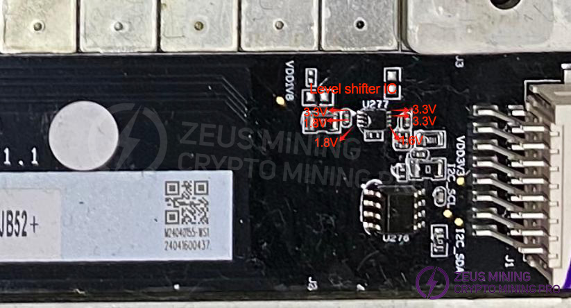
(2) TX signal flow: The signal enters from pin 4 of the connector (3.0V), is converted to 1.8V by level conversion IC U277, and then transmitted from chip #1 to chip #204. The voltage is 0V when the ribbon cable is not connected, and 1.45V-1.8V during operation.
(3) RX signal flow: From chip #204 to chip #1, converted to 3.0V by level conversion IC U277, and then returned to pin 2 of the signal ribbon cable connector to the control board; the voltage is 1.8V when the signal ribbon cable is not connected (there is a 1K pull-up resistor R168 at the last stage), and 1.8V-0V during operation;
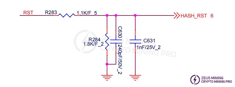
(4) RST signal flow: Enters from pin 5 of the connector (3.0V), is divided to 1.8V by resistors R283 and R284, and then transmitted from chip #1 to chip #204; the voltage is 0V when the signal ribbon cable is not connected, and 1.8V during operation.

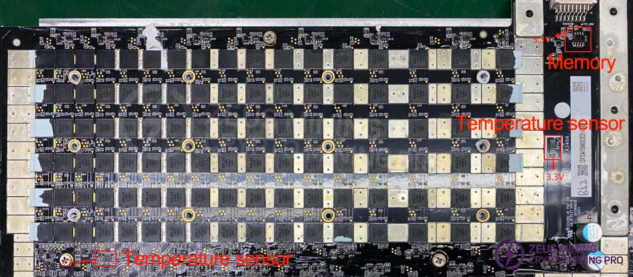
4. Both the temperature sensor and the memory are powered by 3.3V, and the voltage is 0V when the signal cable is not connected.
 5. Level Shifting IC: Uart TX 3.0V→1.8V / Uart RX 1.8V→3.0V, powered by LDO U205 1.8V and the control board 3.0V. When the signal cable is not connected, the 3.3V voltage is 0V (Note: RX has a 1K pull-up resistor to 1.8V on chip 204, so the voltage is 1.8V).

V. Common Malfunctions and Troubleshooting Steps for Hash Boards
1. Phenomenon: Hash board not detected
The reset signal voltage is 0V, and the 34-level voltage domain voltage division is abnormal:
A-1) Locate the two levels with the most considerable voltage division change, and use an oscilloscope to measure whether the clk signal in the higher voltage domain (6 chips) is standard.
A-2) Voltage domain is close to 0V: Disconnect the power and use a multimeter to measure the impedance of each domain. If the impedance is significantly less than 0.8Ω, there is a short circuit in the chip. Remove the chips in this domain one by one to identify the damaged chip.
Reset voltage is 0V, voltage domain voltage division is normal, Reset signal voltage is 1.8V, voltage domain voltage division is abnormal:
Step 1: Check if the boost circuit's VTT voltage (measured across C617 with a multimeter) is the standard 25.8V.
Step 2: Check the 1.8V and 0.85V voltage domains
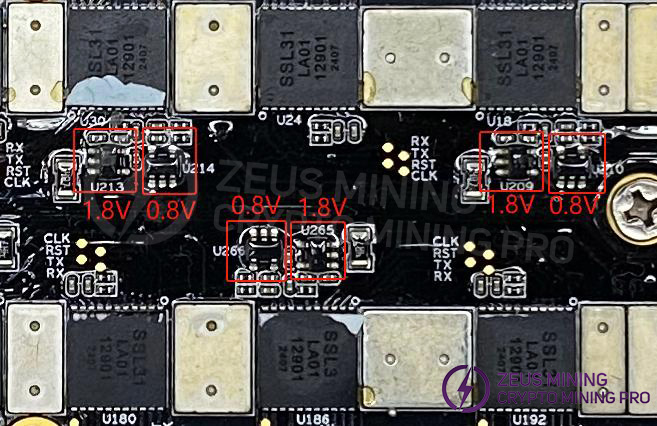
(1) Measure the 1.8V and 0.85V LDO outputs in each domain using a multimeter.
A-1) If the 1.8V LDO voltage is abnormal and the 0.85V LDO voltage is normal: Measure the 0.85V LDO input voltage with a multimeter. If it is around 1.24V, there is likely a short circuit between the 0.85V LDO VIN, EN, and GND pins. Use tweezers to clean the 0.85V LDO input to check for any foreign objects.
A-2) If the 1.8V LDO output is standard and the 0.85V LDO output is abnormal: Measure the CLK/RST/RX/TX signal voltage of each chip in this domain with a multimeter to determine which chip is short-circuited.
A-3) If both the 1.8V and 0.85V LDO outputs are standard, measure the capacitor voltage of the 1.8V and 0.85V power supply pins of each chip in this domain with a multimeter. If there is no 1.8V or 0.85V on the pins, it indicates a poor solder joint on the chip.

Step 3: Check the chip signal output (CLK/RST/RX/TX)
Refer to the voltage range described in the signal flow diagram. If you encounter significant voltage deviations during measurement, compare the values with those of adjacent groups to determine whether the deviation is significant.
2. Phenomenon: Incomplete chip detection on the single board
a) 0 chips detected:
When the repair software log shows a ChipID 0 timeout, first measure the domain voltage and the boost circuit voltage at 25.8V to ensure they are within normal limits, then rerun the repair software and check the software log.
If zero chips are still found, then it will be one of the following situations:
A-1) Use a multimeter to measure whether the LDO 1.8V and 0.85V voltages are standard. If not, it may be that the 1.8V and 0.85V LDO circuits in this domain are abnormal, or the two chips in this domain have poor soldering, or it may be caused by a short circuit in the 0.85V and 1.8V surface-mount filter capacitors.
a-2) Check whether the circuits of U5 and U4 are abnormal, such as poor soldering of the 1.8V/0.85V power supply pins, etc.
a-3) Check whether the first chip has any pins that are not properly soldered (this has been found during repair; after removing the chip, it was found that the pins were not soldered at all).
b) If one chip is found in step a), it means that the first chip and the previous circuits are sound. Use a similar method to troubleshoot the subsequent chips.
c) Software displays chipID x fail: When a specific chip is consistently reported as failing, the reported chip value usually does not change with each test. In this case, repair using the standard method of measuring signal voltages.
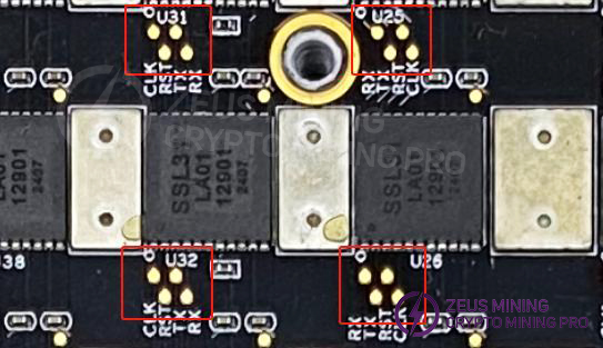
3. Phenomenon: Computing power is NG (not good), there are no defective chips, but the number of cores per chip is <700, which does not meet the standard.
Check the log and replace the two chips with the lowest vld_core_num to restore the overall yield rate to the standard.

PS: Note that abnormal domain voltage can also cause a low number of chipcore cores.
4. Phenomenon: Sensor NG
Repair method: Check the background software to confirm which temperature sensor is reporting an abnormal temperature, and then troubleshoot the corresponding sensor circuit; first, measure whether the power supply to pin 8 of the temperature sensor is 3.3V, and then check whether the SDA and SCL buses are abnormal.
VI. Control board issues causing the following problems:
1. The entire machine does not operate.
(1) Check whether the main voltage output of 5V and the PMU are standard, and whether the crystal oscillator is oscillating normally.
(2) If the voltage is standard, please check the soldering condition of DDR/CPU/EMMC (X-RAY inspection at the production end).
(3) Try reflashing the program using an SD card.
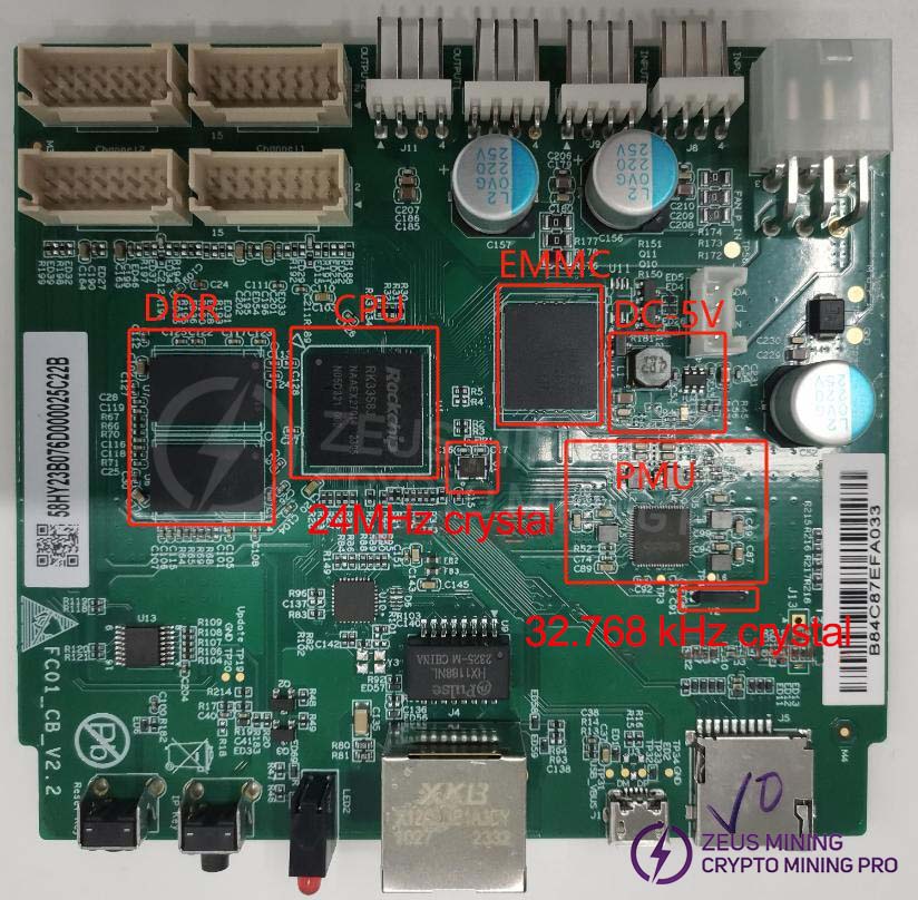
2. The device cannot find an IP address.
This is most likely due to an operating anomaly. Refer to point 1 for troubleshooting.
Prioritize checking the appearance and soldering of network port J4, network transformer U9, CPU, and network card IC U10. Then check whether the power supply to the network card IC and the 25 MHz clock are functioning correctly.
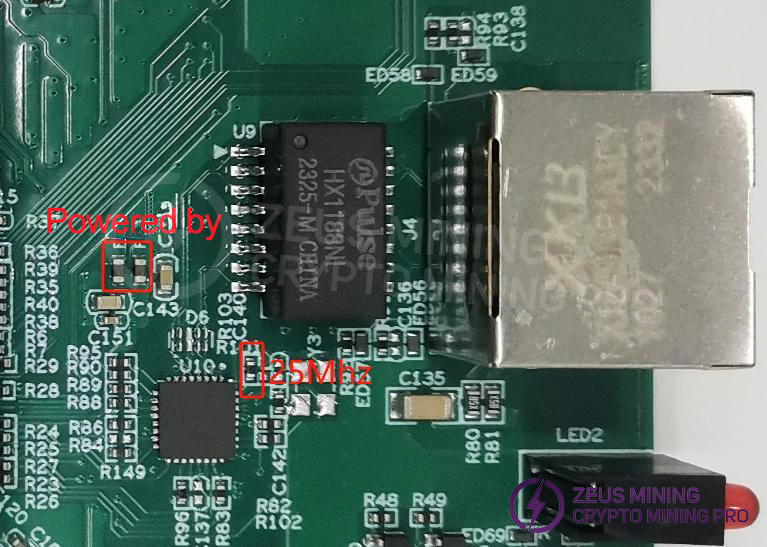
3. The entire machine cannot be upgraded.
Check the appearance and soldering of the network port, network transformer T1, CPU, and EMMC.
4. The entire machine fails to read the hash board or has incomplete connections.
A. Check the ribbon cable connections.
B. Check the components corresponding to the chain on the control board.
C. Check the wave soldering quality of the connector pins and the resistors around the connector interface.
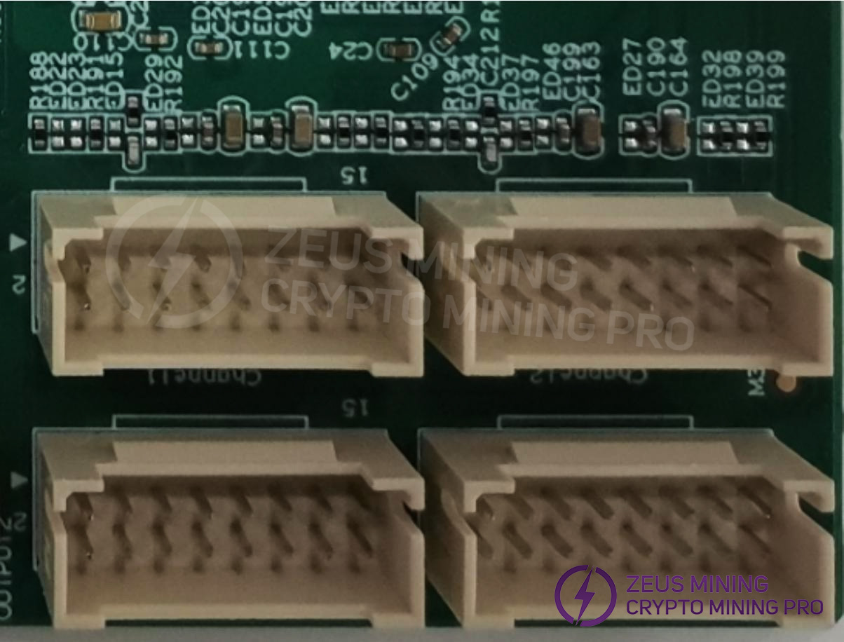
5. Unable to read from memory and sensor.
A. Check the ribbon cable connection.
B. Check the components on the control board corresponding to the chain.
C. Check the wave soldering quality of the connector pins and the resistors around the connector interface.
D. Check the I2C Switch power supply and RST signal.
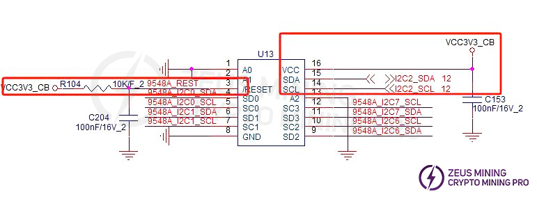
VII. System Malfunction Symptoms
1. Abnormal fan speed display - Check if the fan is working correctly, if the connection to the control board is standard, and if the control board is functioning correctly.
 2. Hash board connection issue: A connection issue means one of the four boards is missing. This usually indicates a problem with the connection between the hash board and the control board. Check the ribbon cable for any open circuits. If the connection is OK, test the individual board to see if it passes. If it passes, the problem is likely with the control board. If the control board fails the test, repair it using the control board repair procedure.

3. Computing board temperature anomaly: This usually refers to high temperature. The monitoring system sets the maximum allowable PCB temperature at 85 degrees Celsius. If the temperature exceeds 85 degrees, the machine will trigger an alarm and shut down, preventing regular operation. This is generally caused by excessively high ambient temperature or a damaged temperature sensor. Fan malfunction can also lead to temperature anomalies.

VIII. Other Important Notes
Repair process flowchart

• Routine Inspection: First, visually inspect the faulty hash board for any PCB deformation or burning; check for any obvious signs of burnt components, component displacement, or missing components. Secondly, test the impedance of each voltage domain for short- and open-circuit conditions. Finally, power on the board and test the voltage in each domain with the Reset signal at 0V and 1.8V, ensuring each voltage is approximately 0.6V.
• After the routine inspection is complete (the short circuit test during routine inspection is essential to prevent damage to chips or other components due to short circuits during power-on), use testing software to test the chips and determine the location of the fault based on the test results.
• Based on the test software log results, start testing the CLK/RST/RX/TX signals and 0.85V, 1.8V voltages near the faulty chip.
• Then, follow the signal flow: RX signal propagates in reverse (204→1), while CLK/RST/TX propagate forward (1→204), using the power supply sequence to locate the abnormal fault point.
• When the faulty chip is located, first take an X-ray to confirm whether there are any cold solder joints. If not, re-solder the chip. The method involves applying flux to the bottom of the chip and heating each chip pin solder joint until it melts, ensuring a tight connection between the chip pins and the solder pads. If the fault persists after re-soldering, replace the chip.
• After repairing the hash board, it must pass the test software test at least twice to be considered a good product. The first test is performed after replacing the components and allowing the board to cool down. After passing the test, set it aside to cool further. The second test is performed after the hash board has fully cooled.
• After repairing the hash board, record relevant information (requirements: SN, PCB version, component location, cause of failure, responsibility for the failure, etc.) for feedback to production, after-sales service, and R&D.
• After recording the information, assemble the board into a complete machine for routine aging testing. • Boards that have been repaired in the production process must be reintroduced into the production line, starting from the visual inspection station.
Dear Customers,
Hello, May 1-5, 2026 (GMT+8) is China's May Day, and international logistics will be suspended. Our company will suspend shipments on the afternoon of April 30, 2026, and resume warehouse shipments on May 6 (GMT+8). We are deeply sorry for the inconvenience caused to you. Thank you for your trust and support.
Best wishes,
ZEUS MINING CO., LTD.