


DG1 Miner Hash Board Repair and Maintenance Guide
I. Preparation of repair equipmentRepair:
1. Materials and Tools:
Solder flux, solder paste, alcohol, anhydrous circuit board cleaning solution, thermal conductive silicone grease, BGA reballing stencil, desoldering wick, RS232/TTL USB to TTL serial port module.
2. Testing Tools:
(1) A DC power supply with a voltage of 15V and a current of 30A is provided for stable power supply to the high-power computing board.
(2) Custom power adapter cables are made using thick 4AWG copper wire, with a length not exceeding 60cm, to connect the DC power supply and the computing board, ensuring efficient power transmission.
(3) The control board is powered by a 12V DC power supply.
3. Equipment:
Adjustable constant-temperature soldering iron (350-380 degrees Celsius), digital multimeter, hot air gun (350-600 degrees Celsius), oscilloscope, network cable.
4. Repair Bench:
The workbench must be properly grounded to prevent the accumulation and conduction of static electricity. The workbench surface should use static-conductive materials, such as conductive rubber or metal, to effectively dissipate static electricity.
II. Repair Requirements:
1. When replacing chips, ensure the process is performed skillfully and meticulously to avoid deforming the PCB board. After replacement, carefully inspect the new component and its surrounding area to ensure there are no potential problems such as open circuits or short circuits.
2. All personnel involved in the repair must have at least one year of repair experience and be proficient in BGA/QFN/LGA and other packaging soldering techniques.
3. The repaired computing board must undergo at least two comprehensive tests to ensure stable performance and no defects.
4. Before use, ensure all repair tools and fixtures are in good working condition, and verify the accuracy of the test software parameters and fixture versions.
5. After replacing the chip, perform chip testing first, and then proceed with functional testing. During testing, ensure the heat sink is properly installed and that the thermal paste is evenly applied. Also, ensure the cooling fan is running at full speed. When using chassis cooling, two computing boards must be placed to create an effective airflow.
6. When measuring signals, be sure to use an auxiliary fan for cooling and keep the fan running at full speed to prevent the computing board from being damaged due to overheating.
7. When powering on the computing board, the negative power supply copper wire must be connected first, then the positive power supply copper wire, and finally the signal cable. When disassembling, the order is reversed: first disconnect the signal cable, then remove the positive power supply copper wire, and finally remove the negative power supply copper wire. Failure to follow this order may damage the U5 chip. Before testing, ensure the repaired computing board has cooled down sufficiently.
8. Pin printing and solder paste application are required to ensure the chip is pre-tinned before being soldered to the PCBA.
III. Test Fixture Manufacturing Method
1. Obtain the DG01 control board debugging and testing fixture.
2. Update the FPGA of the fixture control board: Use the DG01 series test fixture's SD card flashing program to update the FPGA of the control board. After decompression, copy the files to the SD card and insert the card into the fixture's card slot;
Power on and wait for about 1 minute until the control board indicator light flashes twice, indicating that the update is complete; (Failure to update may cause the test to consistently report a specific chip as defective)
3. Prepare the test SD card according to requirements. For single-sided heat sink chip testing, simply decompress the compressed package to create the SD card; for PT1 testing, do not plug in the network cable or barcode scanner.
4. Prepare the test SD card according to requirements. PT2 Patter testing requires an SD card. For PT2 testing, the barcode scanner and network cable must be connected.
The fixture's accompanying clamp should meet the heat dissipation requirements of the computing board and facilitate signal measurement.
1. Obtain the debugging and testing fixture for the DG01 control board.
2. Update the fixture control board FPGA: Use the DG01 series test fixture's SD card flashing program to update the FPGA of the fixture control board. Copy the decompressed files to the SD card and insert the card into the fixture's card slot. Then power on and wait for about 1 minute until the control board indicator light flashes twice, indicating that the update is complete. This step is crucial, as an unupdated fixture may lead to consistent errors during testing, resulting in a false positive for a defective chip.
3. Prepare the test SD card: Prepare the corresponding test SD card according to the test requirements. Simply decompress the compressed package and create the SD card. For PT1 testing, there is no need to insert a network cable or barcode scanner.
4. PT2 Patter testing: For PT2 Patter testing, a corresponding SD card is also required, as shown in the figure. During PT2 testing, ensure that the barcode scanner and network cable are connected to meet the testing requirements.
In addition, to ensure the accuracy and efficiency of the test, the fixture's accompanying clamp should meet the heat dissipation requirements of the computing board and facilitate signal measurement.
IV. Explanation of the Principle
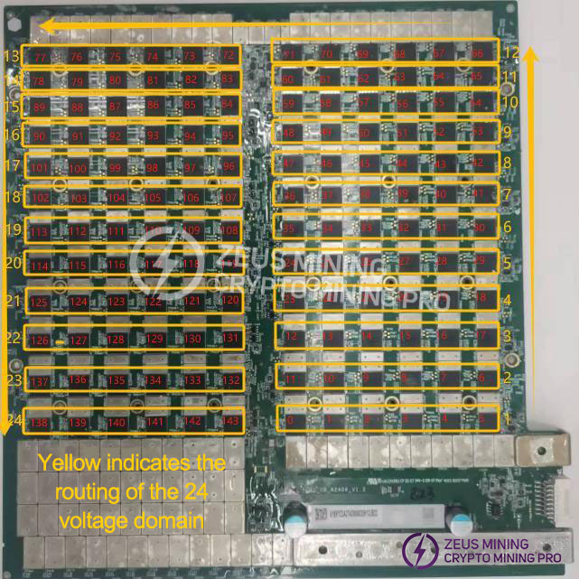
1. The FC01 computing board consists of 144 SSL31 chips, divided into 24 groups (or "domains"), with each group containing 6 ICs. These SSL31 chips operate at a voltage of 0.6V on the computing board.
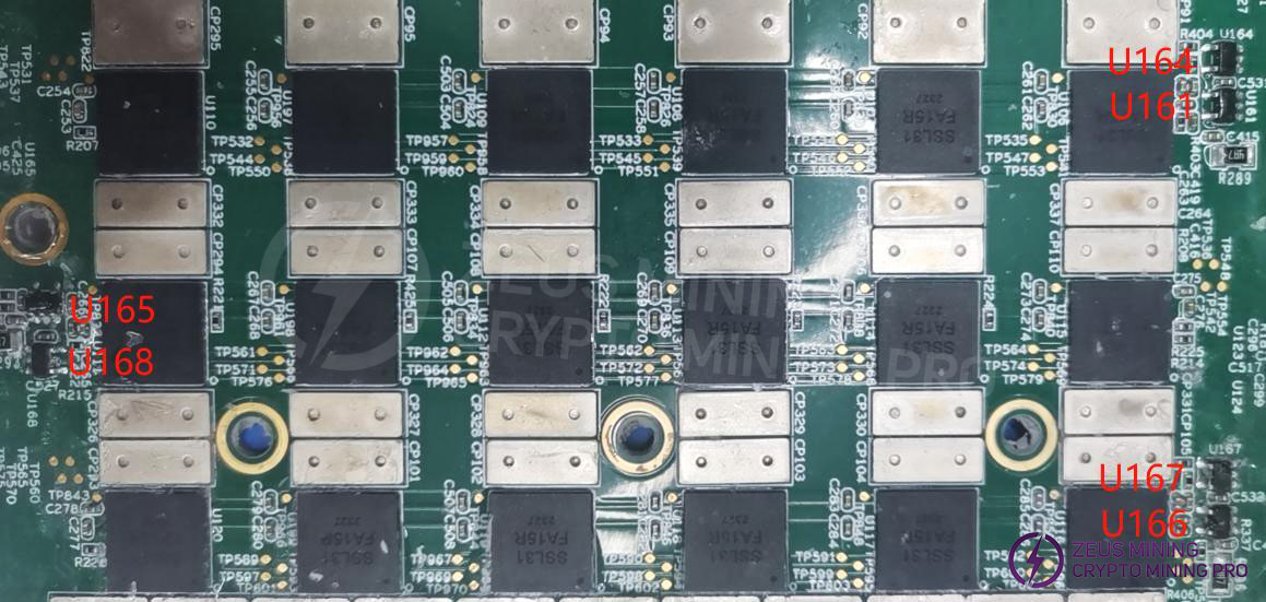
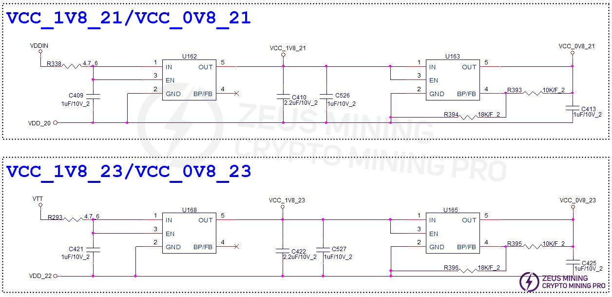
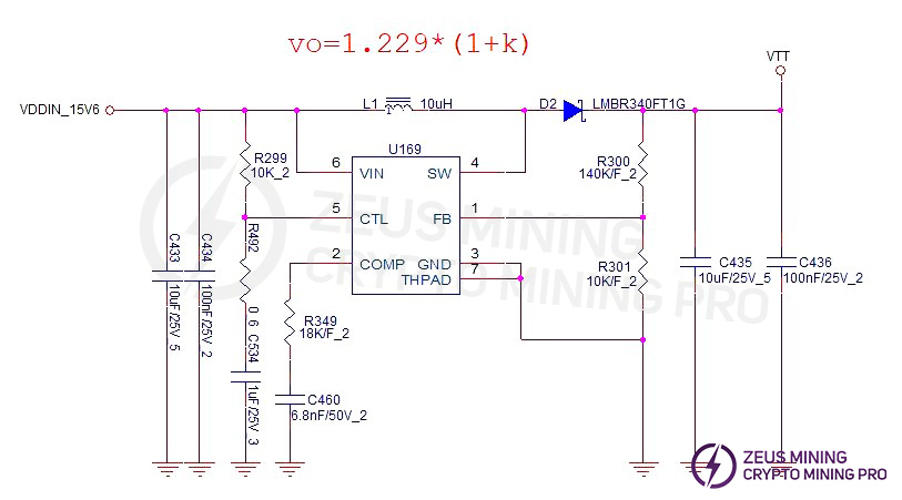
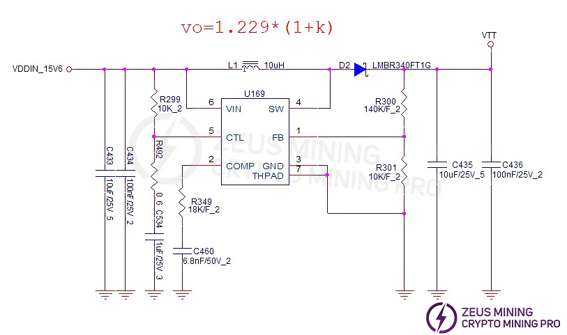
2. Groups 24, 23, and 22 are powered by the boost circuit U169, which outputs 18.4V. This voltage is then further converted by LDOs (U161, U166, U168) to 1.8V and 0.85V. Group 21 directly receives voltage from the VDD14.4V power supply and similarly outputs 1.8V and 0.85V through an LDO. The voltage decreases by 0.6V for each subsequent domain.
3. FC01 Control Board Boost Circuit:
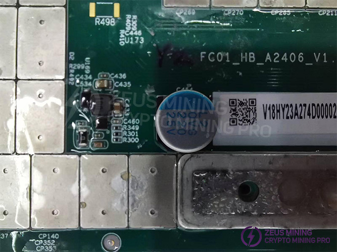
The power supply voltage of 14.4V is converted to 18.4V through the boost circuit, as shown in Figure 4-4.
4. FC01 chip signal flow:
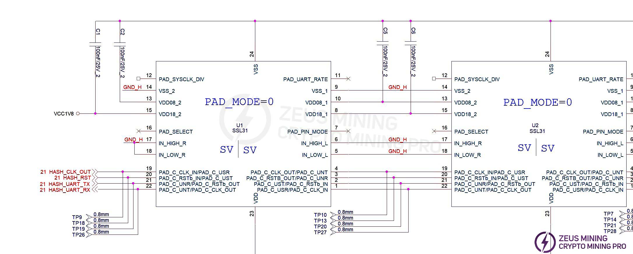
(1) CLK signal flow: A 1.8V (U200 LDO) 25MHz waveform is generated by the X1 active crystal oscillator and provided to all chips from chip #1 to #144 through series resistor R277; the voltage measured by a multimeter is approximately 0.8V-0.9V;
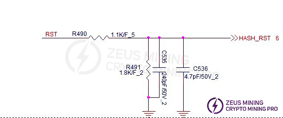
(2) RST signal flow: It enters from connector pin 5 (3.0V), is divided to 1.8V by resistors R490 and R491, and then transmitted from chip #1 to chip #144; the voltage is 0V when the signal cable is not connected, and 1.8V during operation;
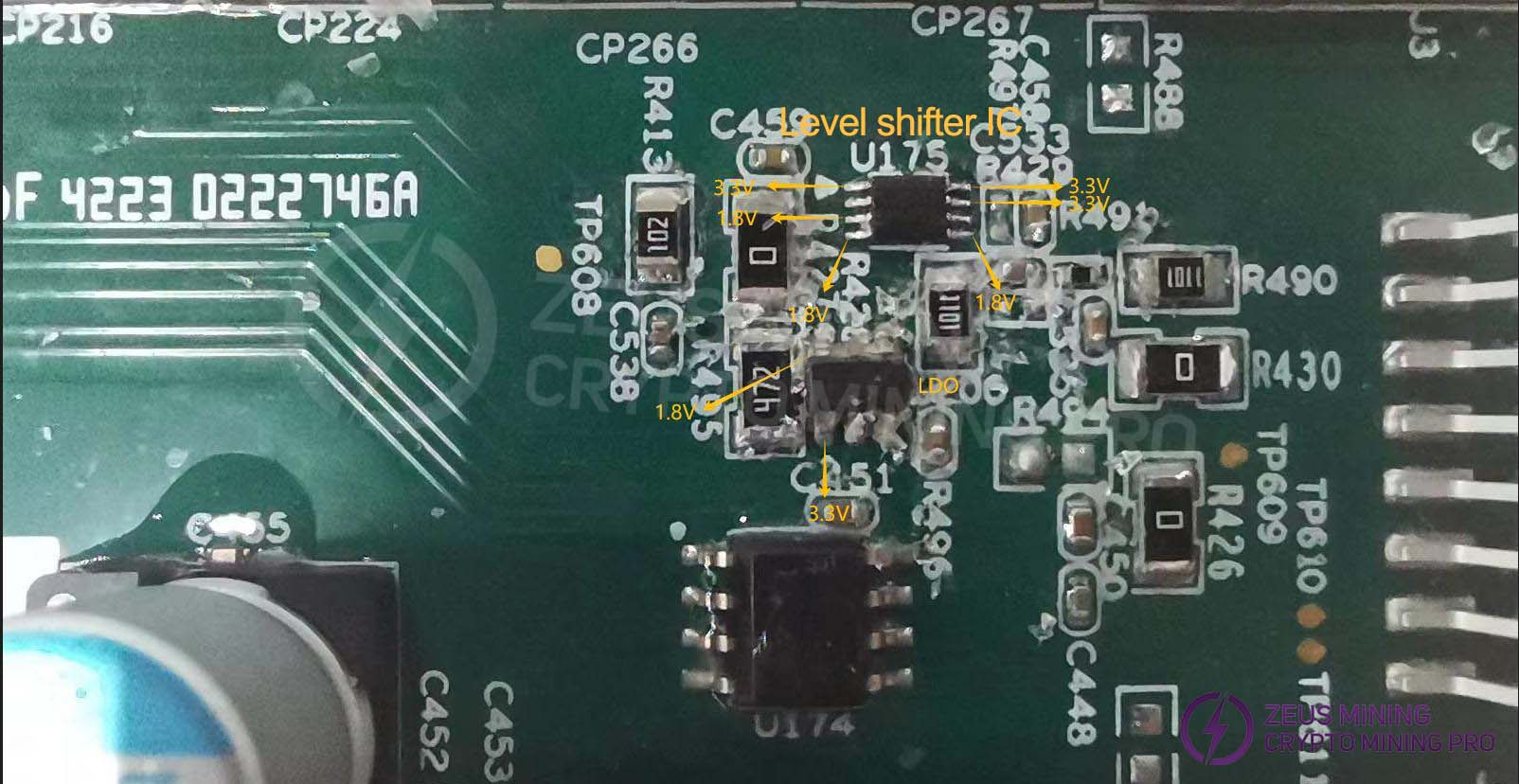
(3) TX signal flow: It enters from connector pin 4 (3.0V), is converted to 1.8V by level shifter IC U175, and then transmitted from chip #1 to chip #144; the voltage is 0V when the signal cable is not connected, and 1.8V during operation;
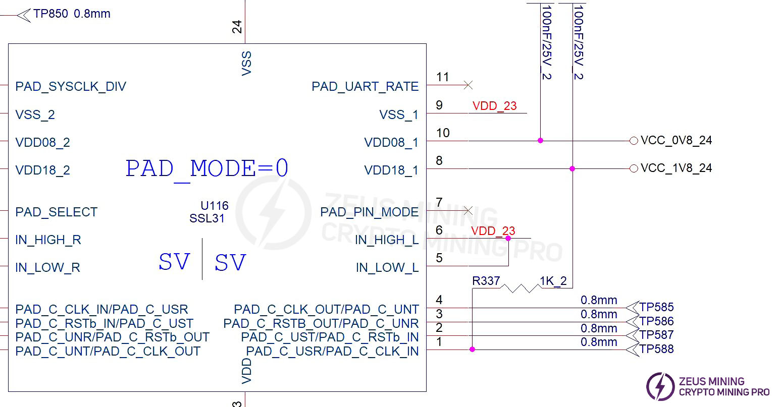
(4) RX signal flow: From chip #144 to chip #1, it is converted to 3.0V by level shifter IC U175 and then returned to the control board via pin 2 of the signal cable connector; the voltage is 1.8V when the signal cable is not connected (there is a 1K pull-up resistor R337 at the last stage), and the voltage is 1.8V-0V during operation.


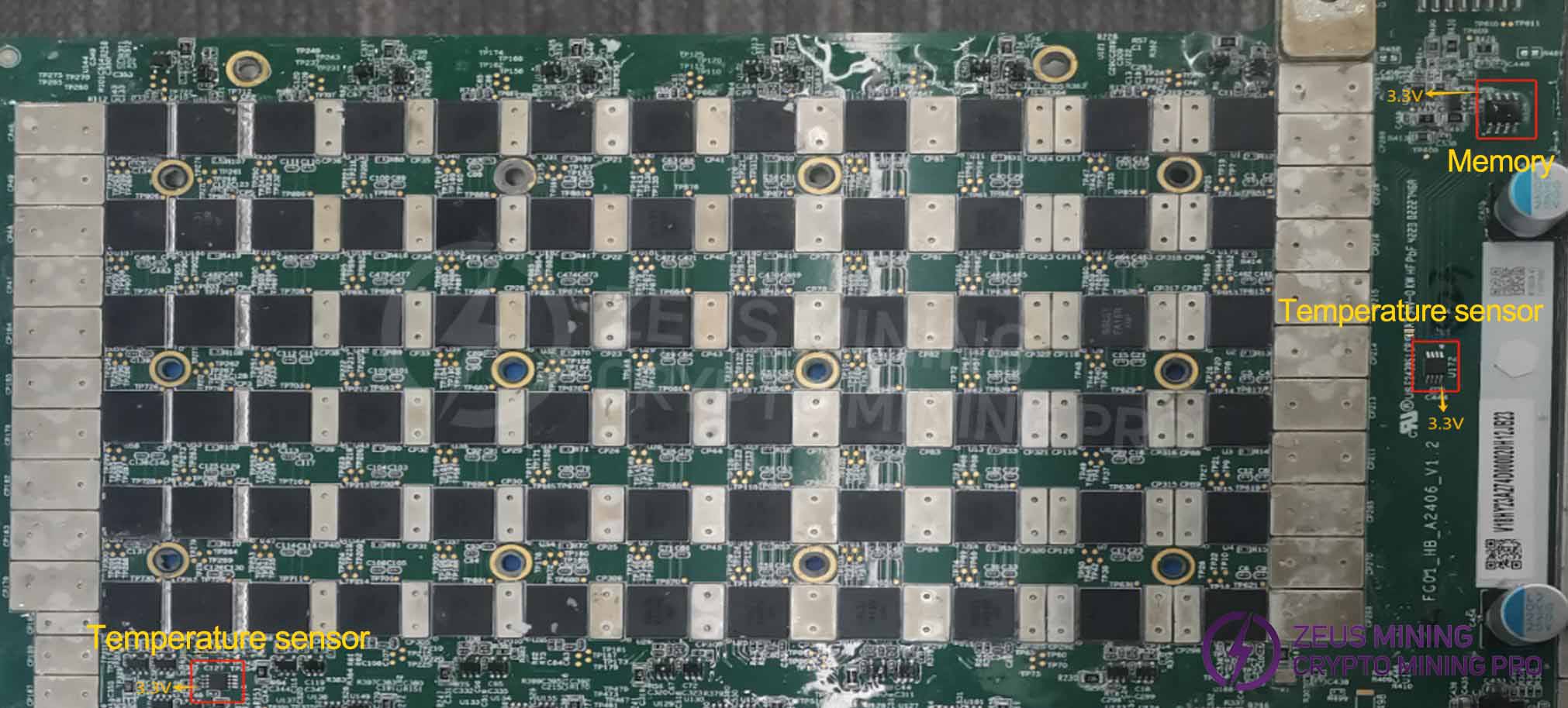
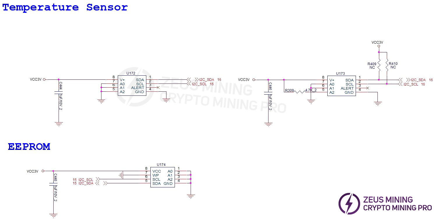
 5. Both the temperature sensor and the memory are powered by 3.3V, and the voltage is 0V when the signal cable is not connected.
6. Level Shifting IC: Uart TX 3.3V→1.8V / Uart RX 1.8V→3.3V, powered by LDO U200 1.8V and the control board's 3.3V supply. When the signal cable is not connected, the 1.8V and 3.3V voltages are 0V (Note: RX has a 1K pull-up resistor to 1.8V on chip #144, so the voltage is 1.8V).

V. Common Malfunctions of Computing Boards and Troubleshooting Steps
1. Phenomenon: Hash board not found
Reset signal voltage is 0V, and the 24-stage voltage divider is abnormal:
a-1) Locate the two stages with significant voltage changes, and use an oscilloscope to measure whether the clk signal in the higher voltage domain (6 chips) is normal.
a-2) Voltage domain is close to 0V: Disconnect the power and use a multimeter to measure the impedance of each domain. If the impedance is significantly less than 0.8Ω, there is a short circuit in the chip. Remove the chips in this domain one by one to identify the damaged chip.
Reset voltage is 0V, voltage divider is normal, Reset signal voltage is 1.8V, voltage divider is abnormal:
Step 1: Check if the boost circuit voltage VTT (measured across C435 with a multimeter) is a normal 18.4V.
Step 2: Check the 1.8V and 0.85V voltage domains
Measure the 1.8V and 0.85V LDO outputs in each domain using a multimeter.
a-1) If the 1.8V LDO voltage is abnormal and the 0.85V LDO voltage is normal: Measure the 0.85V LDO input voltage with a multimeter. If it is around 1.24V, there is likely a short circuit between the 0.85V LDO VIN, EN, and GND pins. Use tweezers to clean the 0.85V LDO input to check for any foreign objects.
a-2) If the 1.8V LDO output is normal and the 0.85V LDO output is abnormal: Measure the CLK/RST/RX/TX signal voltage of each chip in this domain with a multimeter to determine which chip is short-circuited.
a-3) If both the 1.8V and 0.85V LDO outputs are normal: Measure the capacitor voltage of the 1.8V and 0.85V power supply pins of each chip in this domain with a multimeter. If there is no 1.8V or 0.85V on the pins, it indicates a poor solder joint on the chip.


Step 3: Check the chip signal output (CLK/RST/RX/TX)
Refer to the voltage range described in the signal flow diagram. If you encounter significant voltage deviations during measurement, compare the values with those of adjacent groups to make a determination.
2. Phenomenon: Incomplete chip detection on the single board
(1) 0 chips detected:
If the repair software log shows ChipID 0---ChipID 143 fail, first measure the domain total voltage and the boost circuit 18.4V to ensure they are normal. Then configure the software to only detect ChipID 0, and then run the repair software again and check the software log. If it still finds 0 chips, then it will be one of the following situations:
a-1) Use a multimeter to measure whether the LDO 1V8 and 0V85 voltages are normal. If not, it may be that the 1.8V and 0.85V LDO circuits in this domain are abnormal, or the two chips in this domain have poor soldering, or it may be caused by a short circuit in the 0.85V and 1.8V surface-mount filter capacitors.
a-2) Check if the circuits of U5 and U4 are abnormal, such as poor soldering of the 1.8V/0.85V power supply pins, etc.
a-3) Check if the first chip has any pins that are not properly soldered (this has been found during repair; after removing the chip, it was found that the pins were not tinned at all).
(2) If one chip is found in step a), it means that the first chip and the previous circuits are good. Use a similar method to troubleshoot the subsequent chips.
(3) Software displays chipID x fail: When a specific chip is consistently reported as failing, the reported chip value usually does not change with each test. In this case, repair using the normal method of measuring signal voltages.
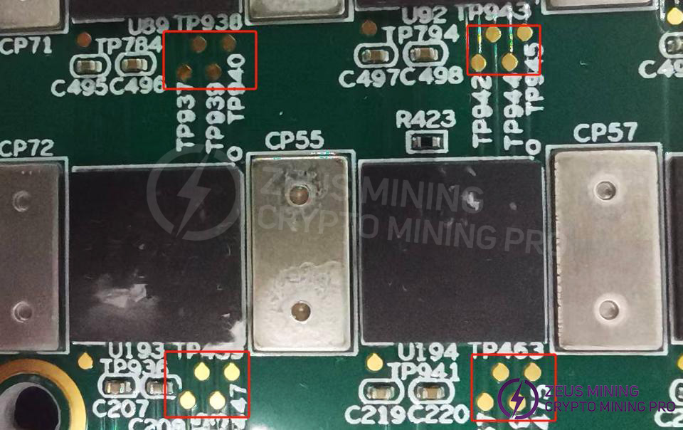
3. Phenomenon: Incomplete nonce data on a single board
The incomplete nonce data is caused by a chip whose characteristics differ significantly from other chips. Therefore, simply replacing this chip will resolve the issue. According to the software log information, the replacement rule is as follows: If the chip's appearance is not damaged, replace the chip with the lowest response rate in each domain.
PS: Please note that both the domain and chip numbers start from 0. Also, abnormal domain voltage can cause insufficient nonce responses from the chip.
4. Phenomenon: Computing power is insufficient (NG), but there are no defective chips; the number of cores per chip is simply less than 700, failing to meet the standard.
Check the log and replace the two chips with the lowest vld_core_num to bring the overall yield rate up to standard.

PS: Note that abnormal domain voltage can also cause insufficient nonce responses from the chip.
5. Phenomenon: Sensor NG
Repair method: Check the software log to identify which temperature sensor is reporting an error, and then troubleshoot the corresponding sensor circuit; first, measure whether the power supply to pin 8 of the temperature sensor is 3.3V, and then check if the SDA and SCL buses are abnormal.
VI. Control Board Malfunction
1. The entire unit is not working.
(1) Check if the 5V and PMU main voltage outputs are normal, and if the crystal oscillator is oscillating properly.
(2) If the voltage is normal, please check the soldering condition of the DDR/CPU/EMMC (production side X-RAY inspection).
(3) Try reflashing the program using an SD card.
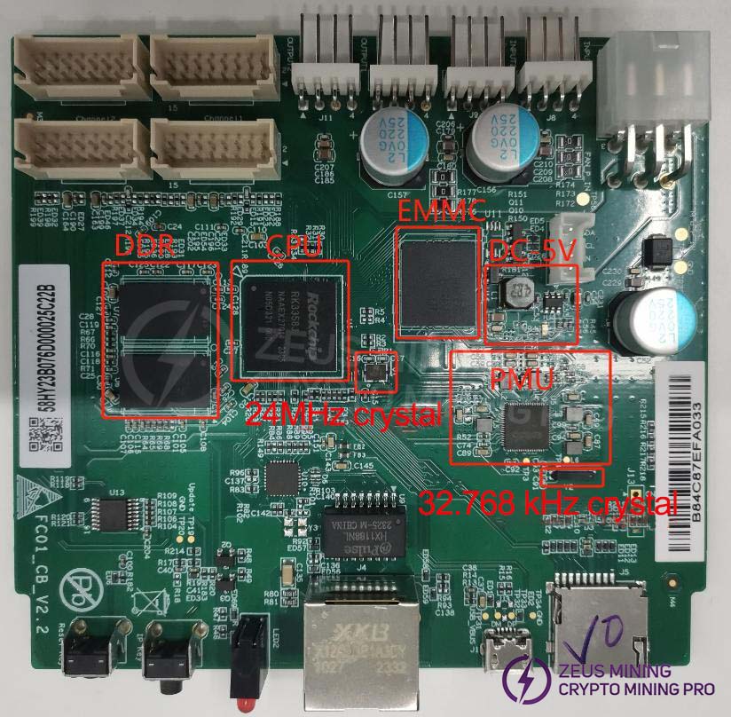
2. Unable to obtain IP address
This is most likely due to a malfunction preventing the device from finding the IP address. Refer to point 1 for troubleshooting.
Prioritize checking the appearance and soldering of network port J4, network transformer U9, CPU, and network card IC U10. Then check the power supply to the network card IC and whether the 25MHz clock is functioning correctly.

3. Unable to upgrade
Check the appearance and soldering of the network port, network transformer T1, CPU, and EMMC.
4. Unable to read hash rate or connection loss
(1) Check the ribbon cable connection status.
(2) Check the components on the control board corresponding to the chain.
(3) Check the wave soldering quality of the connector pins and the resistors around the connector interface.
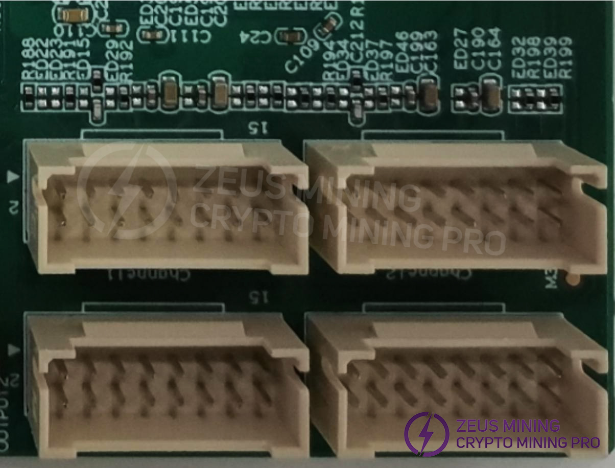
5. Unable to read from memory and sensor
(1) Check the ribbon cable connection.
(2) Check the components on the control board corresponding to the chain.
(3) Check the wave soldering quality of the connector pins and the resistors around the connector interface.
(4) Check the I2C Switch power supply and RST signal.
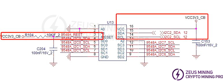
VII. System Malfunction Symptoms
1. Abnormal fan speed display - Check if the fan is working properly, if the connection to the control board is normal, and if the control board is functioning correctly. 2. Hash board connection issue: A connection issue means one of the four boards is missing. This usually indicates a problem with the connection between the hash board and the control board. Check the ribbon cable for any open circuits. If the connection is OK, test the individual board to see if it passes the test. If it passes, the problem is likely with the control board. If the control board fails the test, repair it using the control board repair procedure.
 3. Computing board temperature anomaly: This usually refers to high temperature. The monitoring system sets the maximum allowable PCB temperature at 85 degrees Celsius. If the temperature exceeds 85 degrees, the machine will trigger an alarm and shut down, preventing normal operation. This is generally caused by excessively high ambient temperature or a damaged temperature sensor. Fan malfunction can also lead to temperature anomalies.

VIII. Other Precautions
• Visually inspect the computing board to be repaired, carefully observing its PCB for any abnormalities such as deformation or charring; at the same time, check whether there are obvious burn marks on the components, whether the component positions are shifted, or whether there are missing components. Secondly, conduct a detailed impedance test of each voltage domain to confirm whether there are short circuits or open circuits. Finally, power on the board and check whether the voltages in each domain are around 0.6V when the Reset signal is 0V and 1.8V respectively.
• After preliminary inspection and confirmation (conventional short-circuit detection is particularly crucial, as short circuits may cause damage to the chip or other components when powered on), the chip can be further tested using a test fixture. Based on the software test results, the possible problems can be accurately located and diagnosed.
• According to the test software log results, starting from the area around the faulty chip, test the CLK/RST/RX/TX signals and voltages such as 0.85V and 1.8V.
• The RX signal uses a reverse transmission method, from point 144 to point 1, while the CLK/RST/TX signals use a forward transmission method, from point 1 to point 144. By analyzing the power supply sequence, the abnormal fault point can be accurately located.
• When the faulty chip is located, the chip needs to be re-soldered. The re-soldering method involves applying flux to the bottom of the chip, then heating each solder joint of the chip pins to a molten state to ensure that the chip pins are firmly connected to the solder pads. If the fault persists after re-soldering, replace the chip directly.
• A repaired computing board must pass the test software at least twice to be considered a good product. After replacing parts and completing all repair operations, the computing board needs to cool naturally to room temperature. Then, use the test software for the first test. If the test passes, place the computing board aside for secondary cooling. After ensuring that the computing board is completely cooled, perform the second test. Only when the computing board passes the test software twice consecutively can it be considered a good product.
• After repairing the computing board, make sure to record all relevant information (including SN, PCB version, component location, cause of failure, and responsibility for the failure) for feedback to production, after-sales service, and R&D.
• Aging testing can only be performed after the repair records are completed.
Dear Customers,
Hello, May 1-5, 2026 (GMT+8) is China's May Day, and international logistics will be suspended. Our company will suspend shipments on the afternoon of April 30, 2026, and resume warehouse shipments on May 6 (GMT+8). We are deeply sorry for the inconvenience caused to you. Thank you for your trust and support.
Best wishes,
ZEUS MINING CO., LTD.