


Antminer APW121215A Miner Power Supply Repair Manual
I . Product Appearance
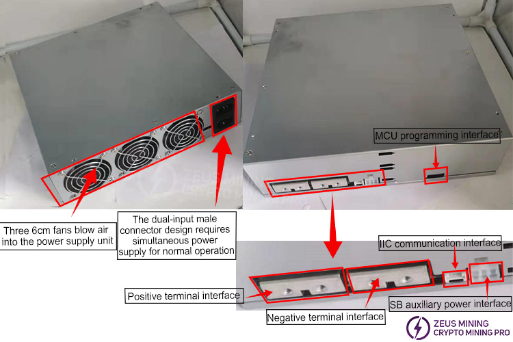
II. Internal Structure
1. Extreme caution is required when inspecting and repairing high-voltage areas to prevent the risk of electric shock.
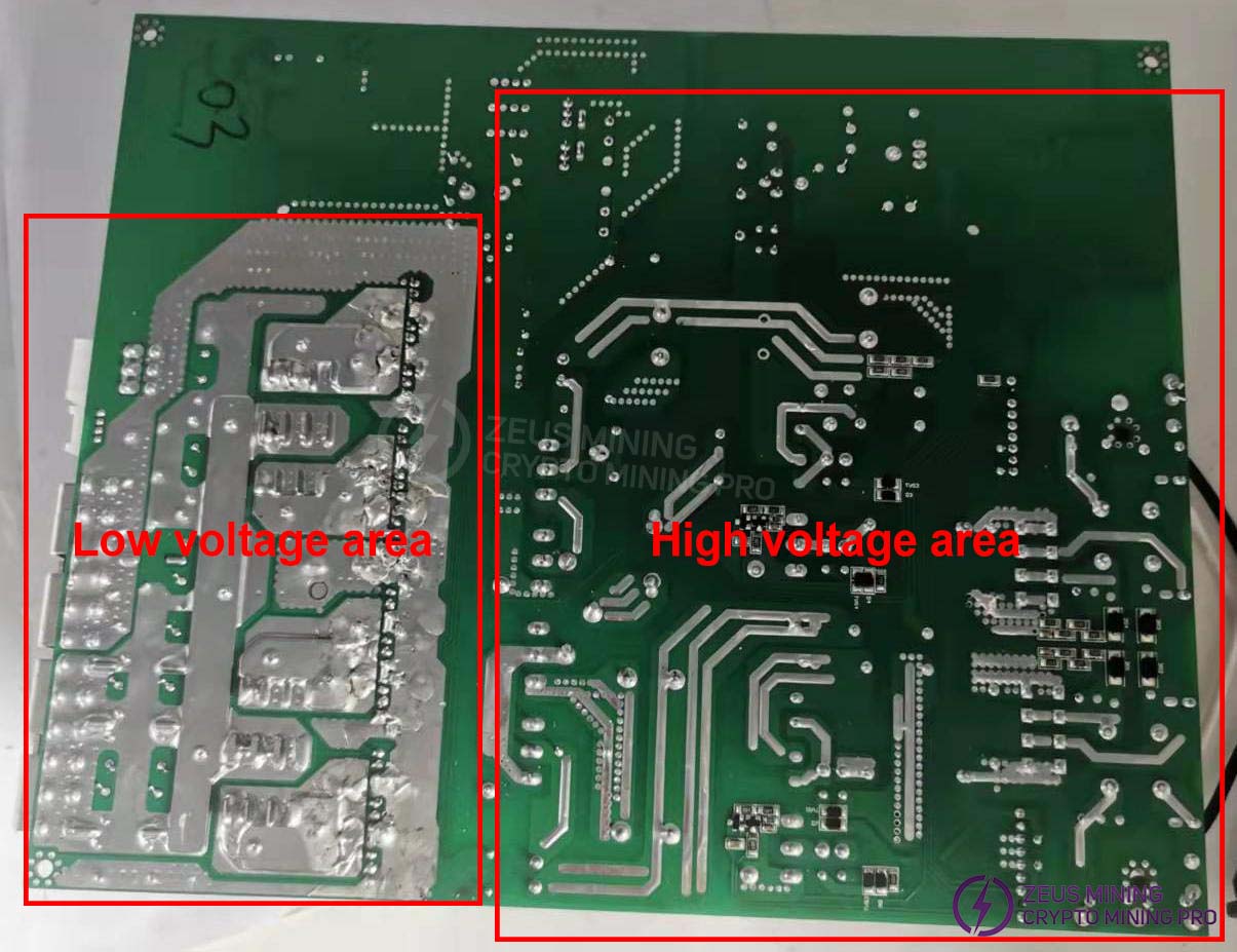
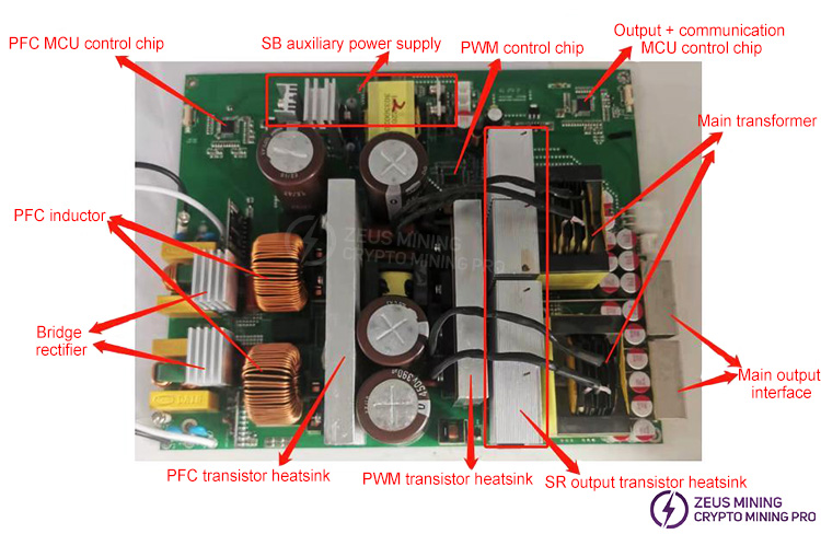
2. Introduction to power supply components
III. Explanation of Working Principle
1. Power supply functional block diagram
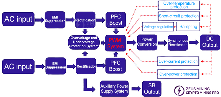
2. Power supply schematic
This power supply's primary circuit consists of two independent PFC stages and requires simultaneous power input to operate correctly. The input voltage range is 180V-300Vac.
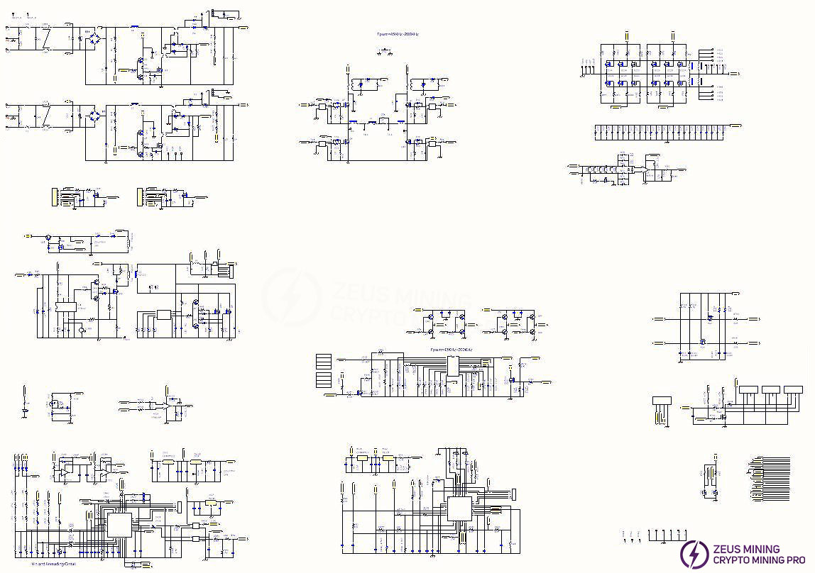
The schematic diagram is attached

IV. Troubleshooting Common Problems
Number | Fault symptoms | reason | Solution |
1 | The fan is not running, and there is no output at OUT2 | Abnormal AC power supply | 1. Check if the AC power cord is functioning properly and if both ends of the plug are securely connected. |
2. Check if there is power in the grid and if the voltage is normal. | |||
2 | The fan is working normally, but there is no output at OUT2 | AC input cable not fully connected | Check if both AC input lines are fully connected and not loose. |
3 | OUT1 has no output | 1. Output short circuit 2. Remote device not powered on | 1. Check if the load is short-circuited. |
2. Check if the host computer sends a power-on signal; low level is active. | |||
4 | The power supply is working intermittently | 1. Output overloa 2. Low input voltage 3. Over-temperature protection | 1. Check if the load is overloaded. |
2. Check if the input voltage is too low or if the power distribution line capacity is insufficient. | |||
3. A. Check if the cooling fan is operating normally. | |||
4. Check if the power supply's cooling air ducts are blocked. | |||
5. Check if the power supply has accumulated excessive dust due to prolonged use. | |||
5 | The output is normal, but the fan is not running | 1. Fan stalled 2. Fan broken | 1. Check if the fan is blocked by debris. |
2. Replace the fan. |
V. Repair
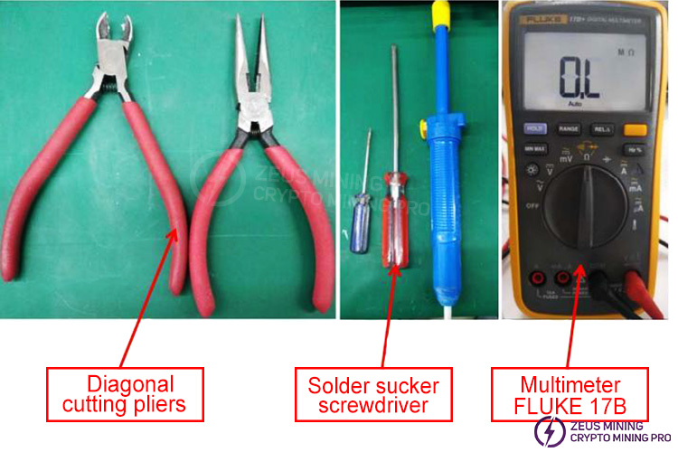
1. Preparation of repair tools
Prepare essential repair tools such as pliers, screwdrivers, tweezers, multimeter, soldering iron, and desoldering pump.
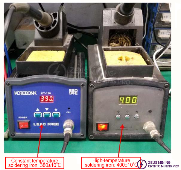
2. Soldering Iron Usage Guidelines
1) When using a soldering iron, the normal temperature should be set at 380±10 degrees Celsius, and the soldering time should not exceed 3 seconds (e.g., when soldering fine component leads or SMD components).
2) When soldering components with heat sinks, the soldering iron temperature can be adjusted to 400±10 degrees Celsius. Special care must be taken to avoid damaging the PCB board or copper traces during soldering.
3) Do not forcibly remove power components before the solder is completely melted or removed, to prevent damage to the PCB board's copper traces.
3. Troubleshooting approach for faulty power supplies
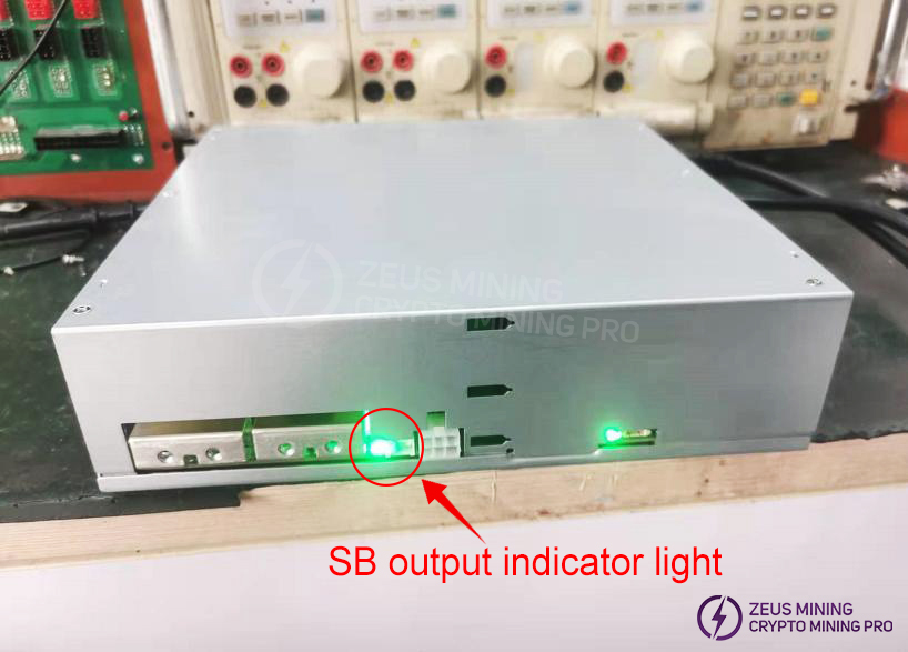
1) After powering on, first confirm if there is an SB output (check if the SB output indicator light is illuminated). The SB output voltage is +12V ±5%.
If the SB indicator light is on, the power supply fan is rotating normally, and the output voltage is within the specified range, then the auxiliary power supply circuit is considered normal; otherwise, it is considered faulty.
No output from SB is usually caused by the following defects:
a. Fuse open circuit
b. SB control chip damaged
c. SB primary MOS damaged
d. SB secondary MOS damaged or short-circuited
e. Power supply diode open circuit or damaged
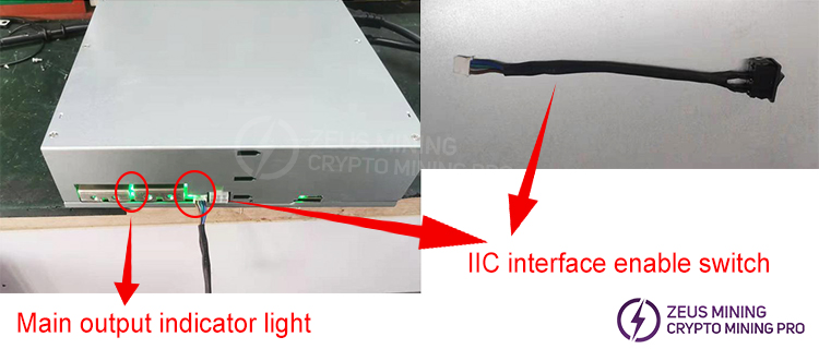
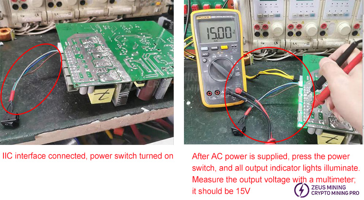
2) After confirming that the SB auxiliary power supply is normal, insert the IIC interface start switch, press the switch to the "I" position, and check if the main output indicator light is lit. (Main output voltage range: 12-15V)
If the main output indicator light is on and the power-on voltage is within the range of 15V ± 1%, the power supply is considered to be functioning normally; otherwise, it is considered to be in a faulty state.
No power-on and no output are mainly caused by the following faults:
a. Abnormal auxiliary power supply
b. Functional protection
c. Abnormal PFC operation
d. Abnormal PWM control system drive
e. Damaged MCU chip or program error
f. Damaged primary transistor
g. Damaged secondary transistor
3) SB and main output are normal; further confirmation is needed to verify whether power supply IIC communication is normal.
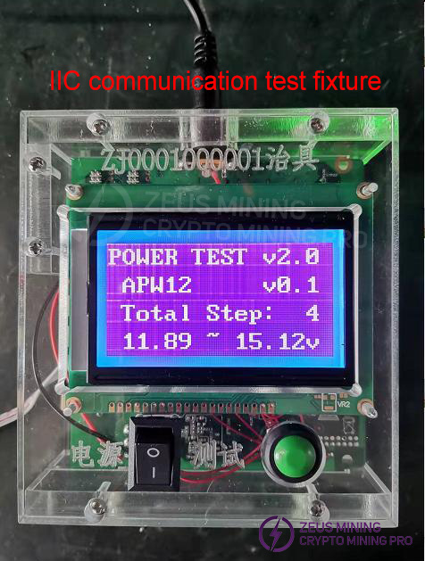
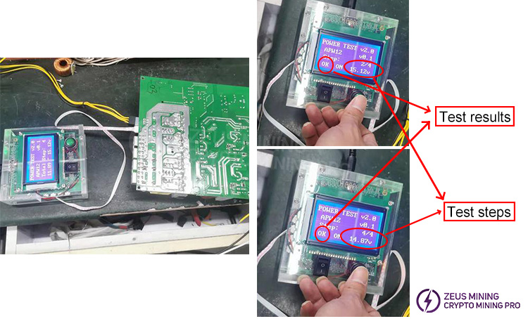
Power on the IIC communication testing fixture and connect the power supply's IIC interface to the fixture. Press the test switch on the fixture. If the fixture displays "PASS," the product is good; otherwise, it is defective.
IIC communication failures can be caused by the following reasons:
a. The IIC communication cable is not conducting or the interface pin arrangement is incorrect.
b. The MCU control chip program is incorrectly programmed.
c. The MCU chip is damaged.
4. Repair & Replacement Materials
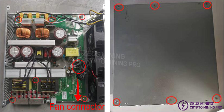
1) Remove the casing
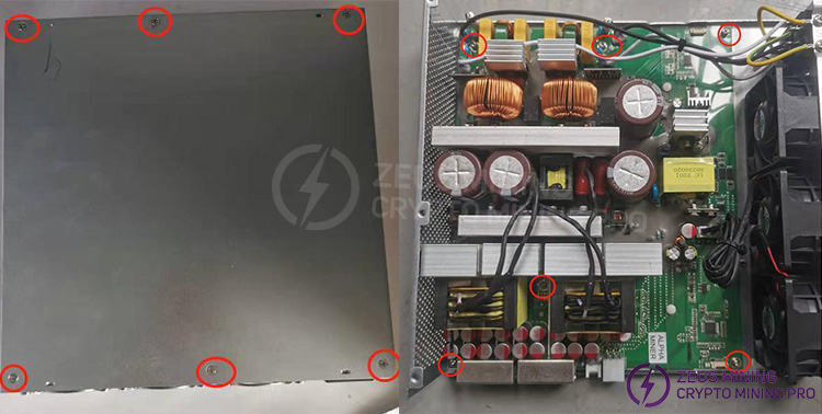
Use a screwdriver to remove the screws securing the case cover and the PCB board (6 screws each).
2) Visual inspection
DIP components:
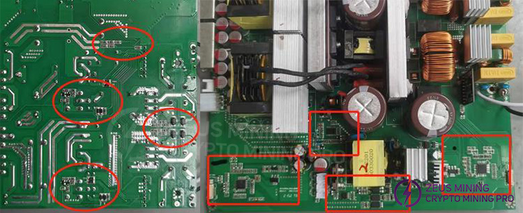
First, visually inspect all components for obvious signs of burning, cracking, or arcing (such as primary transistors, high-voltage capacitors, transformers, fuses, bridge rectifiers, film capacitors, sense resistors, etc.).

SMD components:
Visually inspect the SMD components for any obvious signs of burning, arcing, or burnt and broken copper traces.
3) Multimeter measurement
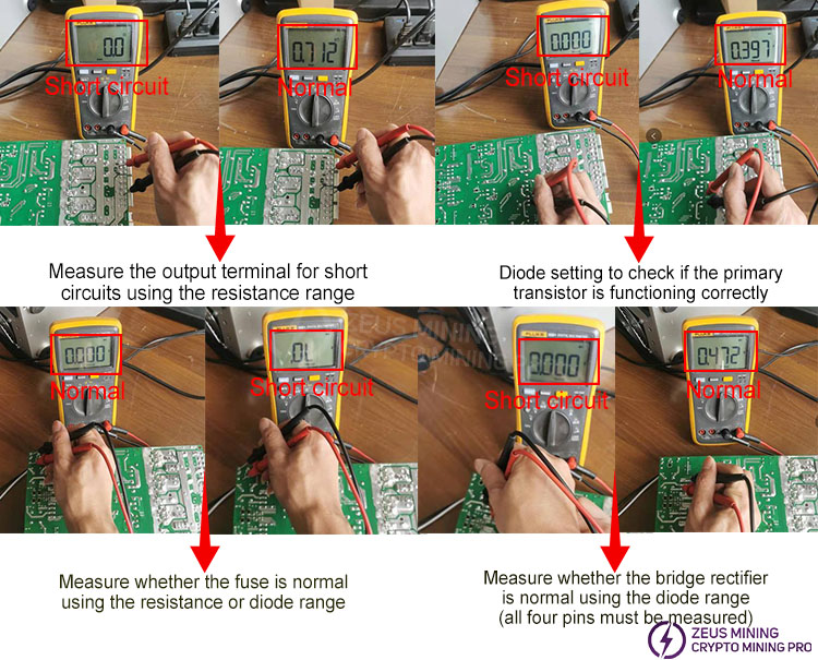
Multimeters are typically used with the "voltage range," "resistance range," and "diode range" settings. For semiconductor materials, the diode range is generally used for measurement (the black probe connects to the negative terminal of the component, and the red probe connects to the positive terminal). The forward voltage drop of a semiconductor is usually in the range of 0.3 to 0.6V for a good component (low-voltage MOSFETs have a voltage drop of around 0.1V), otherwise, it is considered short-circuited or open-circuited. MOSFETs can also be measured using the "resistance range," with the black probe connected to ground and the red probe connected to the gate (G) terminal of the MOSFET; the measured resistance should not be less than 1K ohms.
4) Voltage measurement
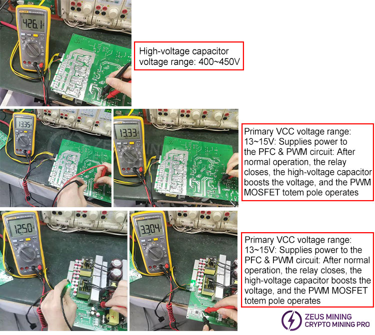
After verifying that all primary transistors are functioning correctly using a multimeter, apply AC power to avoid damage to the primary transistors that could lead to a device failure. Once AC power is applied, the auxiliary power supply circuit will operate first, providing the VCC voltage. This VCC voltage then powers other circuits, allowing them to function. The power supply contains high-voltage components; therefore, extreme caution is necessary during operation. Non-professional repair personnel should not attempt to disassemble the device!
5) Replacement of defective parts
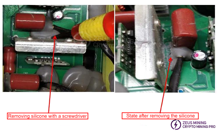
Use a tool to clean off the silicone residue from the part.
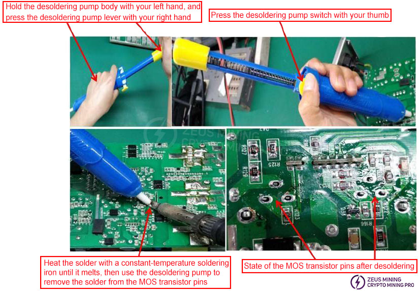
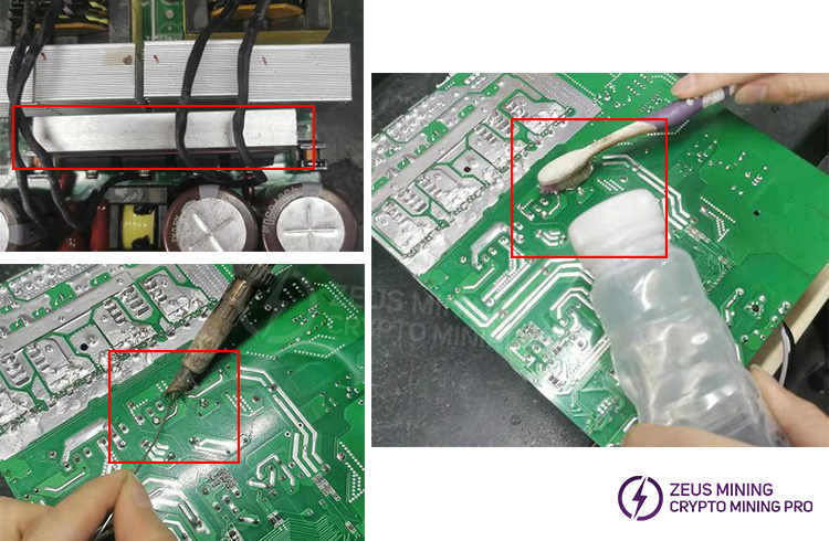
Use a soldering iron and desoldering tool to remove all the solder from the pins of the faulty component (as shown in the diagram). Do not forcibly pull out the component pins before all the solder is removed, as this may break the PCB copper traces or damage the PCB vias, leading to circuit discontinuity.
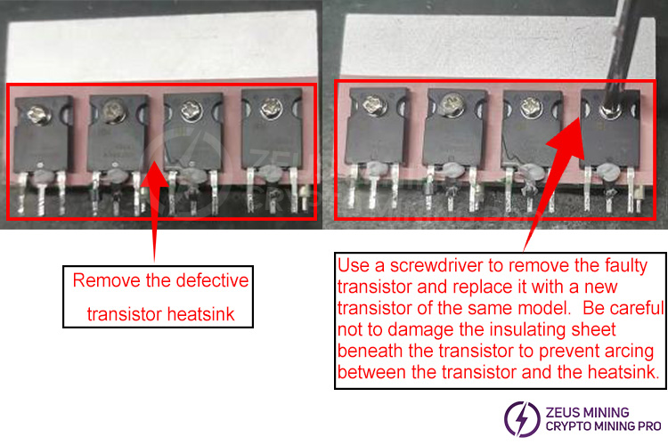
After removing the heatsink, use a multimeter to check for damage to the SMD components around the transistor pins. Replace any damaged components.
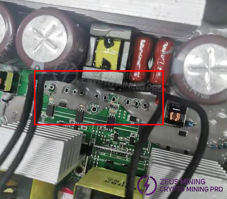
Assemble the heatsink with the replaced transistors onto the PCB board, ensuring that each transistor pin protrudes through the PCB board hole; there should be no bent or missing pins. Solder each transistor pin with a soldering iron, ensuring the solder is full and rounded, without any open solder joints, cold solder joints, or missing solder joints. After soldering, clean the solder surface with board cleaner to remove any contaminants, and check other solder joints for any remaining solder balls.
VI. Testing and Verification
1. Output test
2. IIC Communication Test
Connect the communication fixture to the power supply's IIC interface. Press the test button once; the test fixture should display "OK." Press the test button again; the test fixture should display "Step 2 OK." There are a total of four test steps.
VII. Assembly
Assemble the repaired power supply into the case (ensure the MYLAR insulation sheet in the case is not missing or damaged), and tighten the screws on the PCB board. Plug the fan cable into the corresponding connector, and finally close the case cover and secure it with screws.
Dear Customers,
Hello, May 1-5, 2026 (GMT+8) is China's May Day, and international logistics will be suspended. Our company will suspend shipments on the afternoon of April 30, 2026, and resume warehouse shipments on May 6 (GMT+8). We are deeply sorry for the inconvenience caused to you. Thank you for your trust and support.
Best wishes,
ZEUS MINING CO., LTD.