Date: 2017.10.30
Document Type: Maintenance Plan
Contents of this booklet: Mainly tells about D3 hash board. How to use the test fixture to accurately locate the various faults of the hash board.
Scope: Applicable to all D3 Production, after-sales, outsourcing maintenance site.
I. Maintenance platform requirements1. Constant temperature soldering iron ( 350 degrees to 400 degrees). The tip soldering iron tip is used for soldering small patches such as chip resistors and capacitors.
2. The portable desoldering gun is used for chip disassembly and welding. Be careful not to heat it for a long time to avoid PCB blistering.
3. APW3 power supply ( Output 12V, 133A Max ) is used to test and measure the hash board.
4. Multimeter fluke 15b+, D3 test fixture ( conditionally configurable oscilloscope).
5. Flux solder paste, washing water, and absolute alcohol; Washing water is used to clean up the flux residue and appearance after repair.
6. Plant tin fixture, Plant tin steel mesh, Solder paste; When replacing a new chip, The chip must be tinned.
7. Antminer thermosetting adhesive, used to reattach the heat sink after repair.
II. Operational requirements1. Maintenance personnel must have specific electronic knowledge, More than one year of maintenance experience, and proficiency in QFN package soldering technology.
2. After repairing, you must test the hash board more than twice, and it can pass!
3. Pay attention to the operation method when replacing the chip. After replacing any parts, the PCB board has no obvious deformation. Check the replacement parts and the surrounding parts for open circuit and short circuit problems
4. Determine the maintenance station object and the corresponding test software parameters and test fixtures.
5. Inspection tools, Whether the fixture, can work normally.
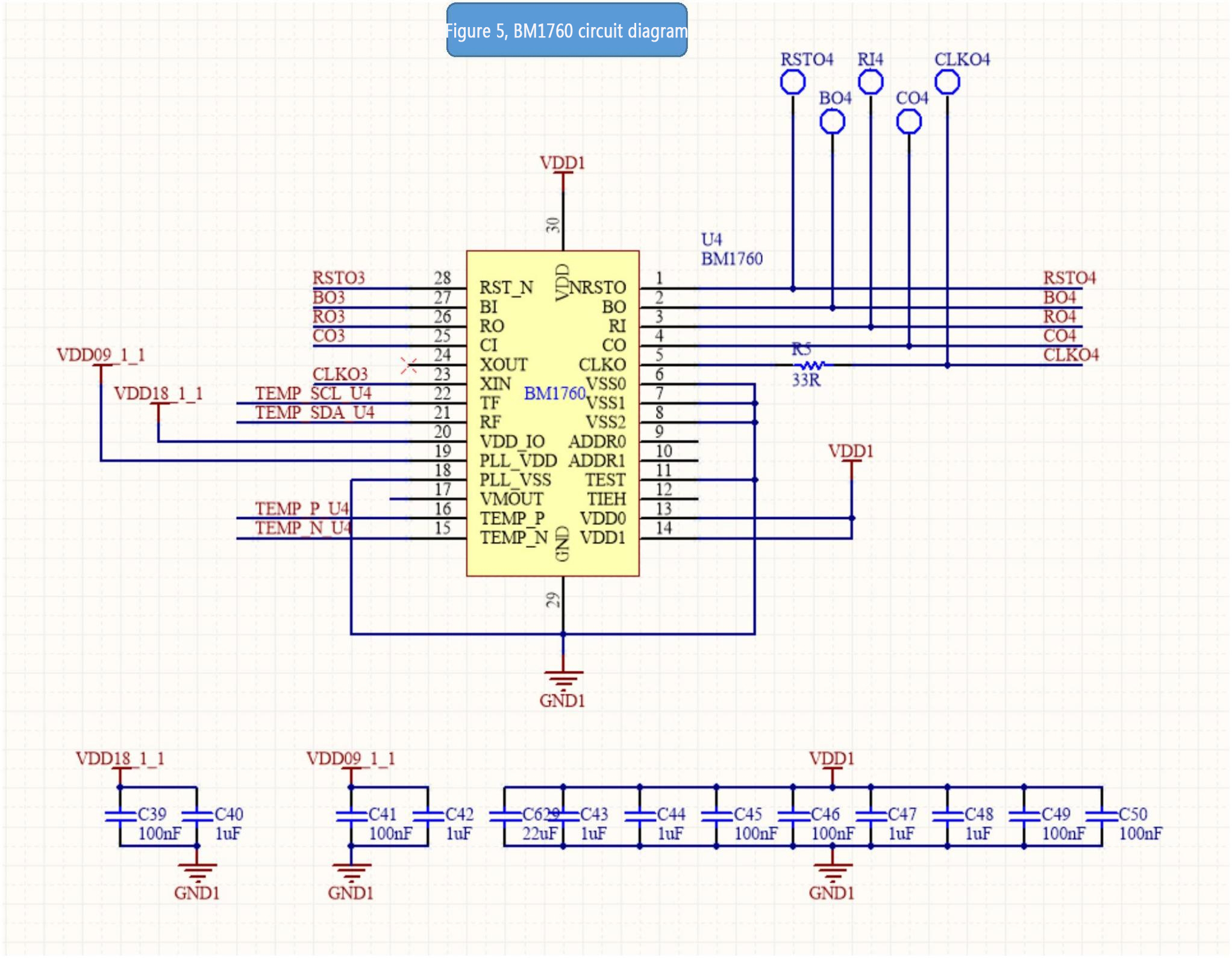
III. Principle and structure1. D3 comprises 10 voltage domains in series. Each voltage domain has 6 BM1760 chips; There are 60 BM1760 chips on the whole board.
2. BM1760 chip has a built-in buck diode. The specified pin of the chip determines the function of the step-down diode.
3. BM1760 clock is a 25M single crystal oscillator, In series from the first 1 Chip to the last chip.
4. D3 each chip has an independent small heat sink on the back. The small heat sink on the back is fixed on the back of the IC with Antminer thermosetting adhesive after the initial test of the board. After the repair and replacement chip has passed the test, It is necessary to apply Antminer thermosetting adhesive on the heat sink and heat it to fix it.
Key point analysis: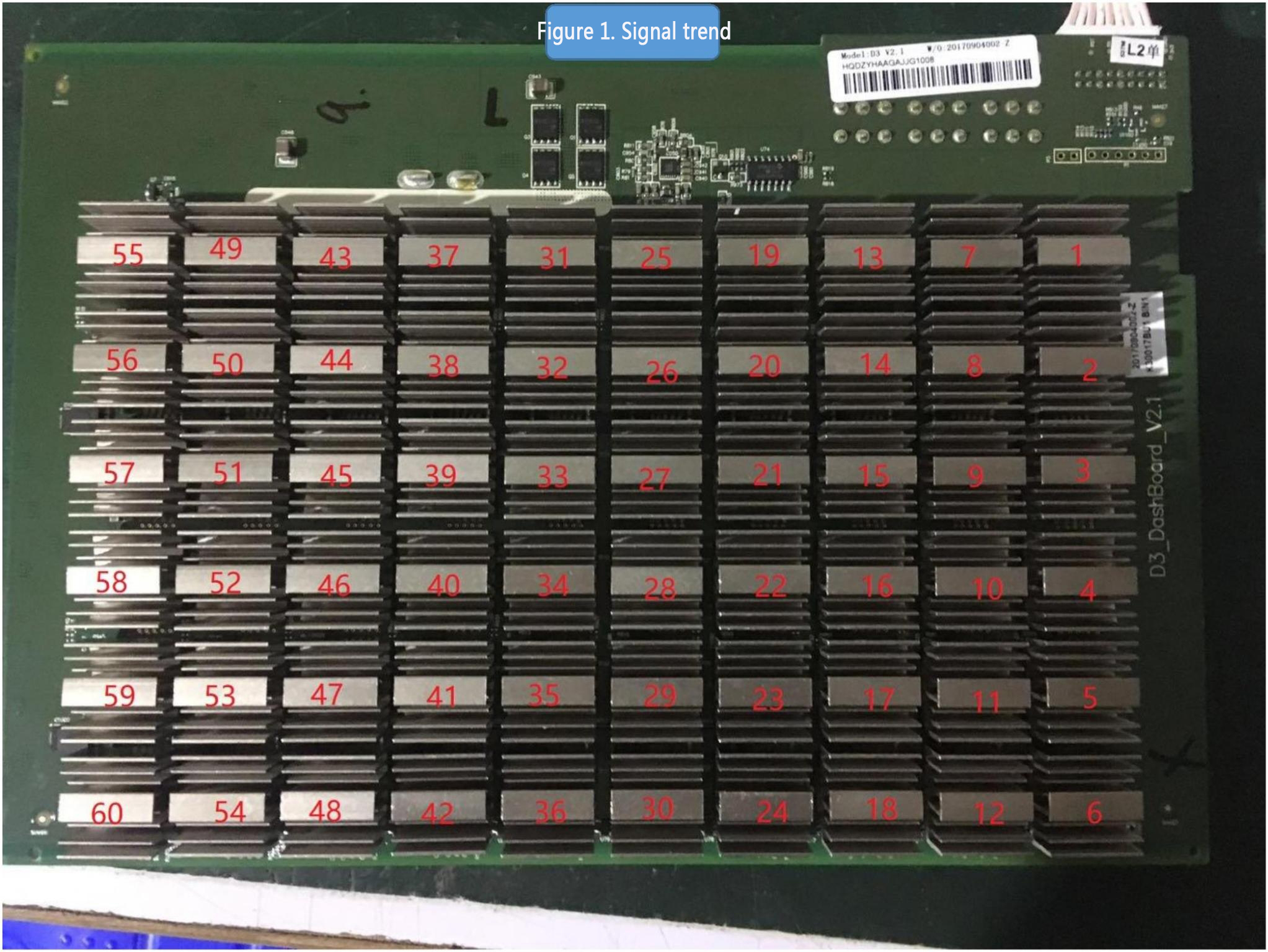
CLK signal flow direction is generated by Y1 25M crystal oscillator and is transmitted sequentially from chip 1 to chip 60; the voltage is 0.9V in both standby and operation.
The TX (CI, CO) signal flows in from pin 11 of the IO port, and then transmits sequentially from chip 1 to chip 72; when the IO line is not inserted, the voltage is 0, and the voltage is 1.8V during operation.
RX (RI, RO) signal flow direction, return from chip 72 to chip 1, and then return to the control board from pin 12 of the IO port; when the IO signal is not inserted, the voltage is 1.8V, and the voltage is also 1.8V during operation.
BI (BI, BO) signal flow direction, pull low level from chip 1 to 72; when the IO line is not inserted, it is 0V when in standby, and it is a pulse signal of about 0.3 during operation.
The RST signal flows in from pin 15 of the IO port, and then is transmitted from chip 1 to chip 60; when the IO signal is not inserted, it is 0V when in standby and 1.8V when in operation.
2. The following figure shows the critical circuits on the front of the D3 hash board.1) Test points between each chip:
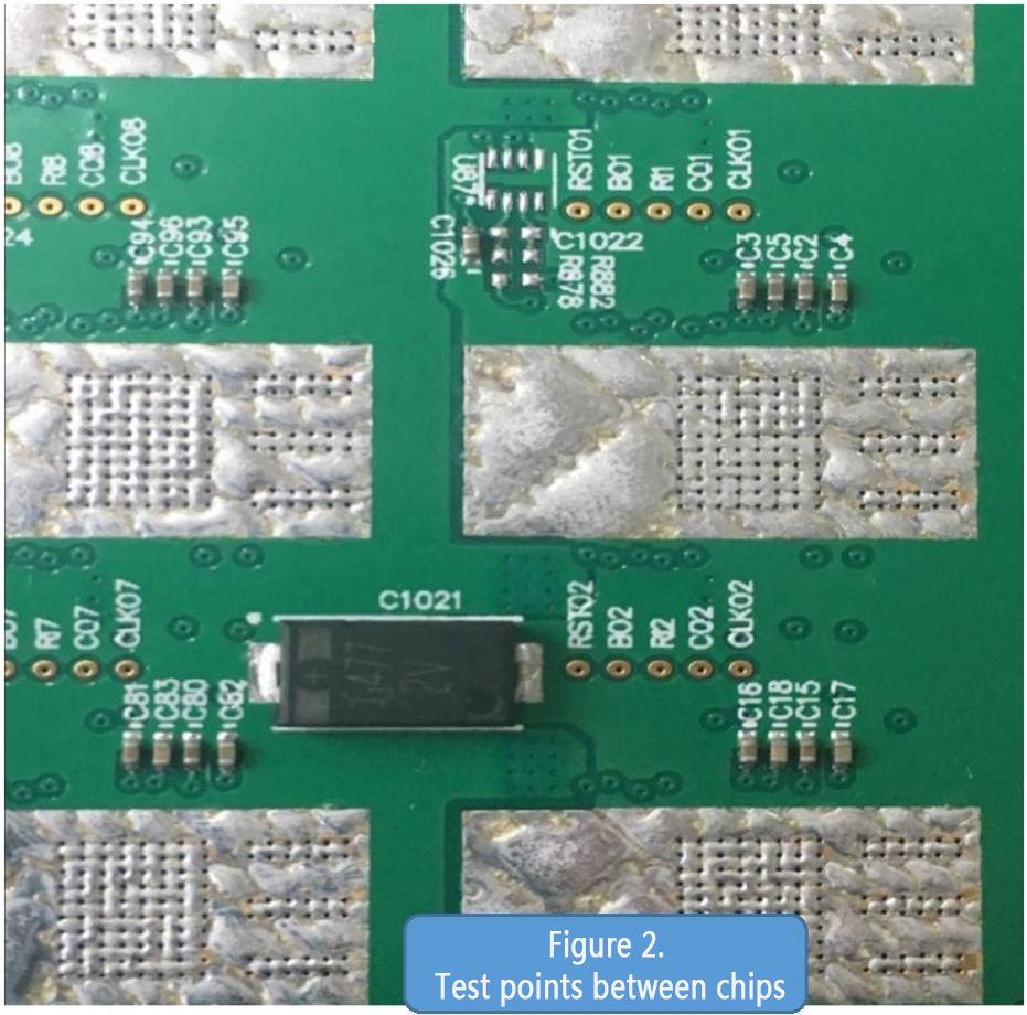
When repairing, the test point between test chips is the most direct fault location the way. The arrangement of the test points of the D3 hash board is RST, B0, RI (RX), C0 (TX), CLK signals.
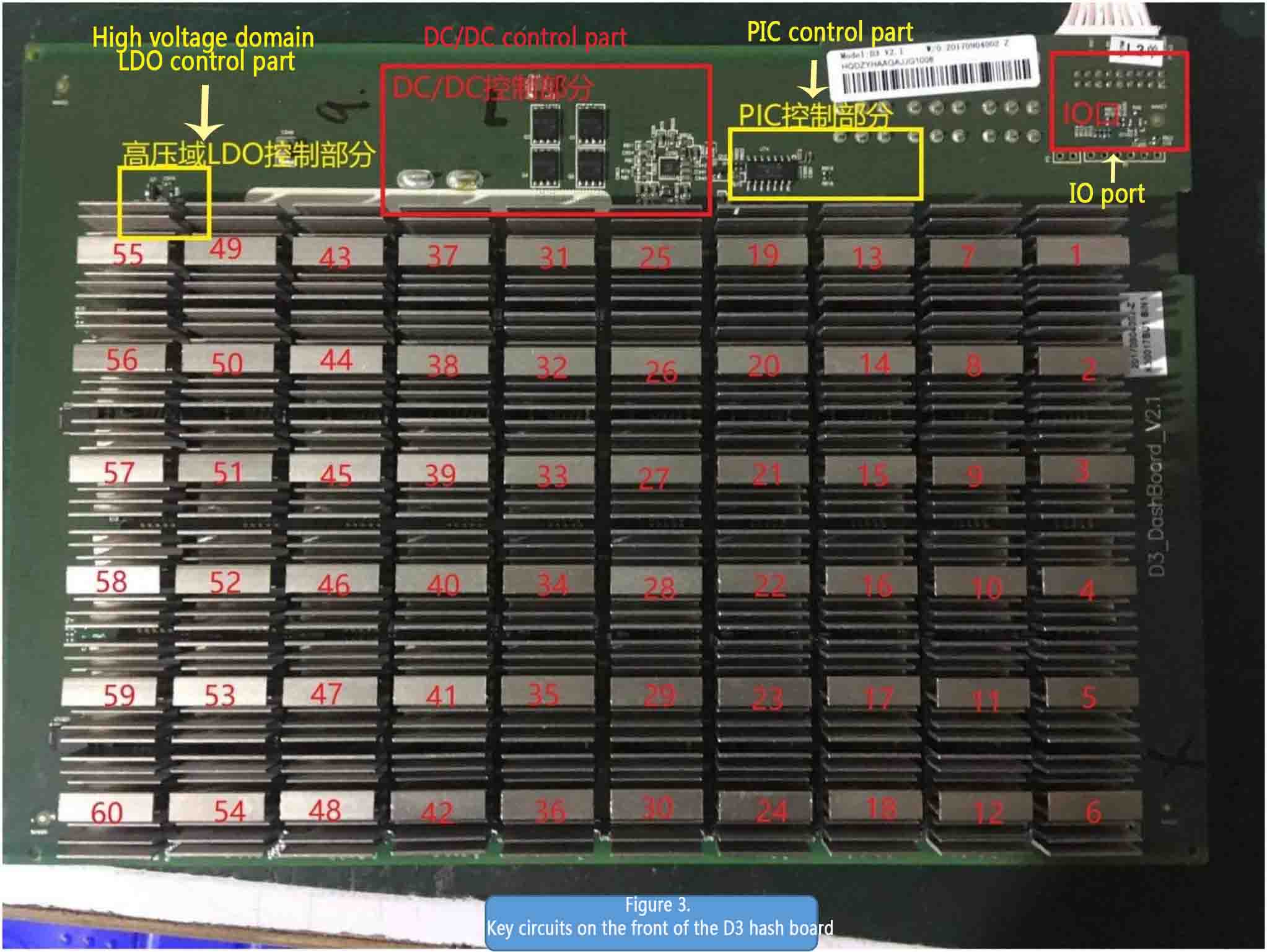
2) Voltage domain: The whole board has 10 voltage domains, and each voltage has 6 chips. Each of the 6 chips in the same voltage domain is powered in parallel and then connected with other voltage domains. The circuit structure is shown in Figure 4 below:
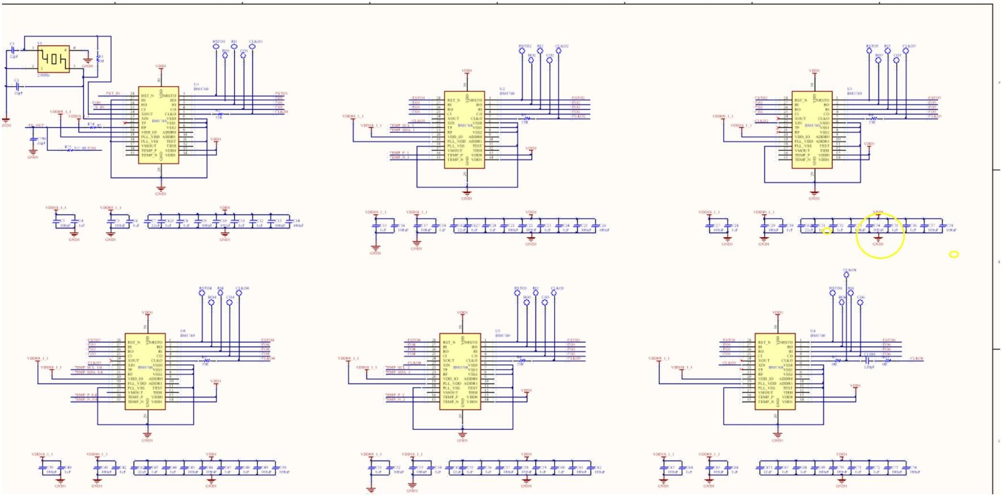
Principle analysis of voltage domain single chip (as shown below5, Figure 6 )
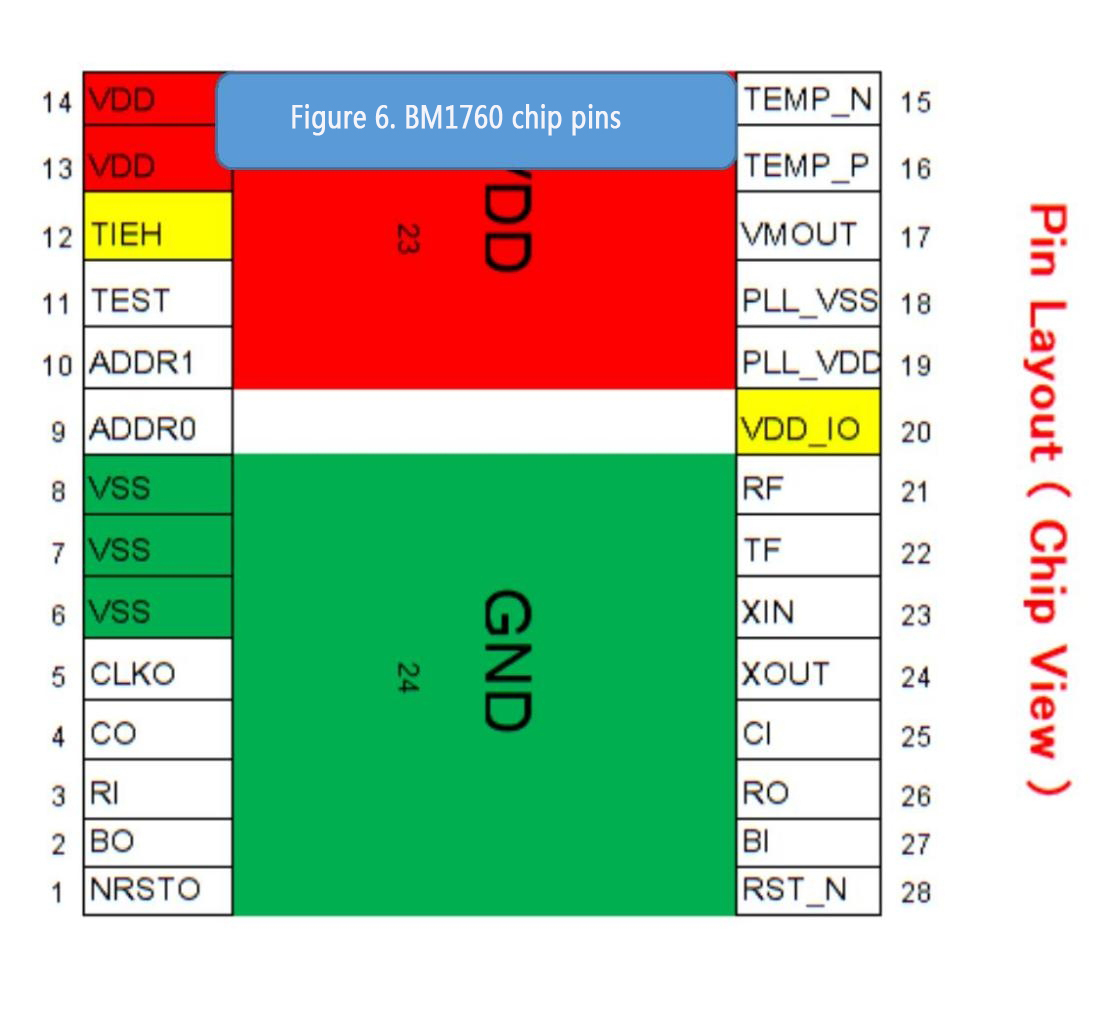 ● The above is the function of each pin of the BM1760 chip
During maintenance, the main test points are 10 test points before and after the chip (5 before and after the chip: CLK, CO, RI, BO, RST); CORE voltage; LDO-1.8V, PLL 0.9V, DC-DC output.
Detection method:1) When the IO line is not inserted, and only 12V is inserted: the DC-DC output is about 8.0V. The test point must have CLK 0.9V, RI 1.8V voltage, and all other test voltages are 0;
2) Insert the IO line. When the test button is not pressed, there is no voltage output for DC-DC and boost. After that, PIC started to work. At this time, after the DC-DC output tool test program sets the voltage in sequence, the tool outputs WORK, and the chip returns the calculated random number. At this time, the average voltage of each test point should be:
CLK: 0.9VCO: 1.6-1.8V. When the tool has just sent WORK, the DC level will be pulled down because of the negative polarity of CO. The instantaneous voltage is about 1.5V.
RI: 1.6-1.8V. If the voltage is abnormal or too low during operation, the hash board will be abnormal, or the hash rate will be 0.
BO: 0V when no calculation is performed. During operation, there will be pulse jumps between 0.1-0.3V.
RST: 1.8V. Each time you press the test button of the tool, a low-level reset signal will be output again.
When the test mentioned above point status and voltage is abnormal, please estimate the fault point based on the circuit before and after the test point.
It can be seen from the chart above:
CLK signal: input from pin 23 of the chip and output from pin 5. When connecting across voltage domains, it is connected from pin 5 to pin 23 of the next chip through a 100NF capacitor connection.
TX signal: input from pin 25 of the chip and output from pin 4;
RX signal: returned by the chip from pin 3 and output by pin 26;
BO signal: input by the chip 27 pin and output by pin 2;
RST signal: input by the chip 28 pin and output by pin 1.
Test the signal voltage of each chip, CORE voltage, LDO-1.8OV, PLL-0.9V, and other voltages:
CORE: 0.8V. When the voltage is abnormal, it is usually the CORE of the chip in the voltage domain is short-circuited
LDO-1.80: 1.8V. When the voltage is abnormal, the chip LDO-1.8O is short-circuited or open.
PLL-0.9: 0.8V. When the voltage is abnormal, the PLL-09V power supply of a particular chip in its voltage domain is short-circuited.
3. IO port definitionIO is composed of 2X9 pitch 2.0 PHSD 90-degree in-line double row. The pin definitions are shown in Figure 8 below:
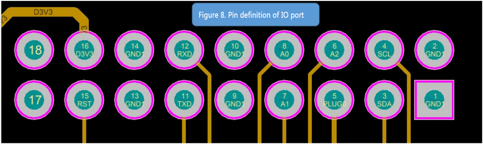
As shown in FIG:
1, 2, 9, 10, 13, 14 feet: It is GND.
3, 4 feet (SDA, SCL): The I2C bus of the DC-DC PIC connects the communication between the control board and the PIC. The control board can read and write the PIC data through it, thereby controlling the operation status of the hash board.
5 feet (PLUG0): It is the identification signal of the hash board. This signal is pulled from the hash board by a 10K resistor to 3.3V, so this pin should be high when the IO signal is plugged in.
6, 7, 8 pins (A2, A1, A0): PIC address signal.
11, 12 feet (TXD, RXD): It is the channel of the hash rate at the 3.3 ends of the hash board, which becomes TX (CO) and RX (RI) signals after being divided by resistors. The levels of the pins of the IO port are both 3.3V. After dividing the voltage through the resistor, it becomes 1.8V.
15 feet (RST): The 3.3V end of the reset signal becomes a 1.8V RST reset signal after being divided by resistors.
16 feet (D3V3): Supply the 3.3V power supply for the hash board. The 3.3V is provided by the control board, mainly to provide the working voltage for the PIC.
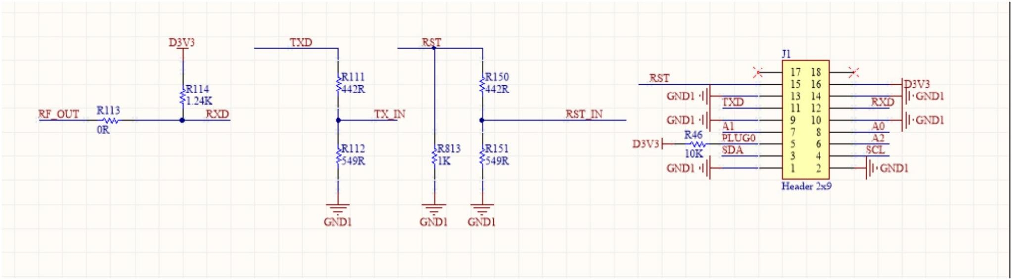
TX_IN voltage is 1.8V
RST_IN voltage is 1.8V
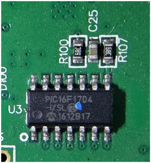
he PIC control part is composed of PIC16(L)F1704. As shown in Figure 13 and Figure 14, the device that stores the frequency information and voltage value of the hash board chip can also be used to control the DC-DC output voltage of the hash board.
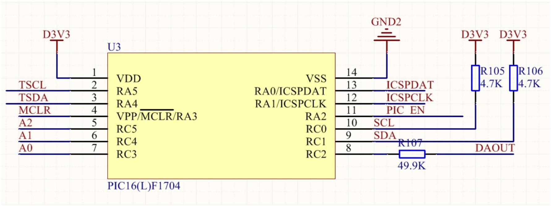
When PIC is working, it needs to control and send a heartbeat signal every minute. With the heartbeat information, the PIC will work for one minute and then shut down. PIC pin 1 is VDD 3.3V, 14 is GND, pins 9 and 10 are the I2C bus that connects the IO port to the control board, pins 5, 6 and 7 are the PIC address; pin 4 is PIC 3.3V; Pin 8 is the FB input of the PIC output, used to control the DC-DC voltage; Pin 11 is the EN signal output by the PIC, which controls the DC-DC working state.
5. DC-DC circuitIt is composed of LM27402SQ and CMOS tube TPHR9003NL. As shown in Figure 15 and Figure 16 below:
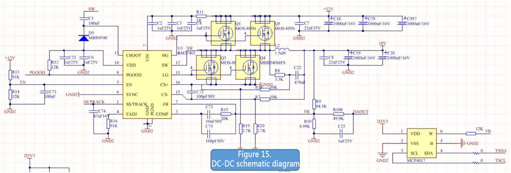
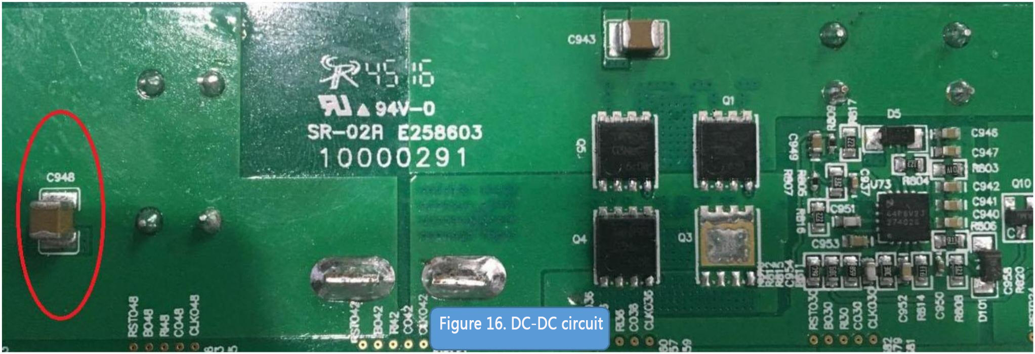
DC-DC output voltage test point is both ends of capacitor C948
When the DC-DC voltage is abnormal, first check whether the PIC voltage value is the same as the DC-DC output voltage through the printed information of the tool; if not, please replace the small capacitor around the LM27402SQ first;
If the DC-DC has no output, please check the EN voltage of R13 and R14 is about 1V, R11 voltage is 12V, whether the PIC works abnormally, and whether the PIC can normally receive the I2C signal of the control board.
6. 1.8V and 0.9V circuit composition1.8V-LDO is composed of 1.8VLDO SPX5205M5_L_1_8.
As shown below:
SPX5205M5 pins 1 and 3 are input, and pin 5 is 1.8V output;
The PLL-0.9V voltage is obtained by dividing the voltage of LOD-1.8 through two resistors. (The location of the LDO is under the heat sink. We can see it in actual maintenance by removing the heat sink, similar to L3+, S9).
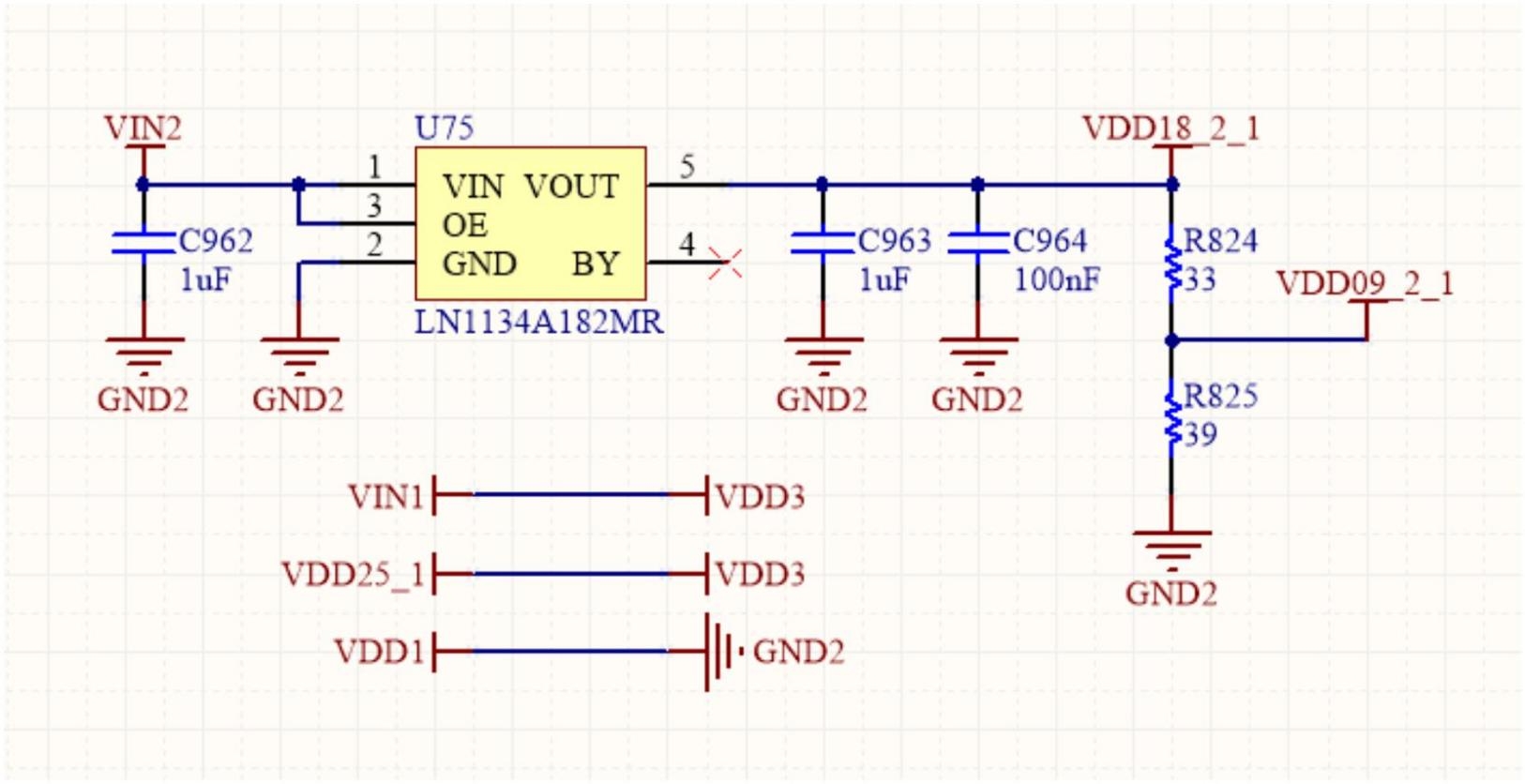
Note: The two LDOs U82 and U83 have EN control functions. If these two LDOs do not have voltage output, please check whether pin 3 of the component is 1.8V. If it is not 1.8V, please check the high-voltage domain LDO control part.
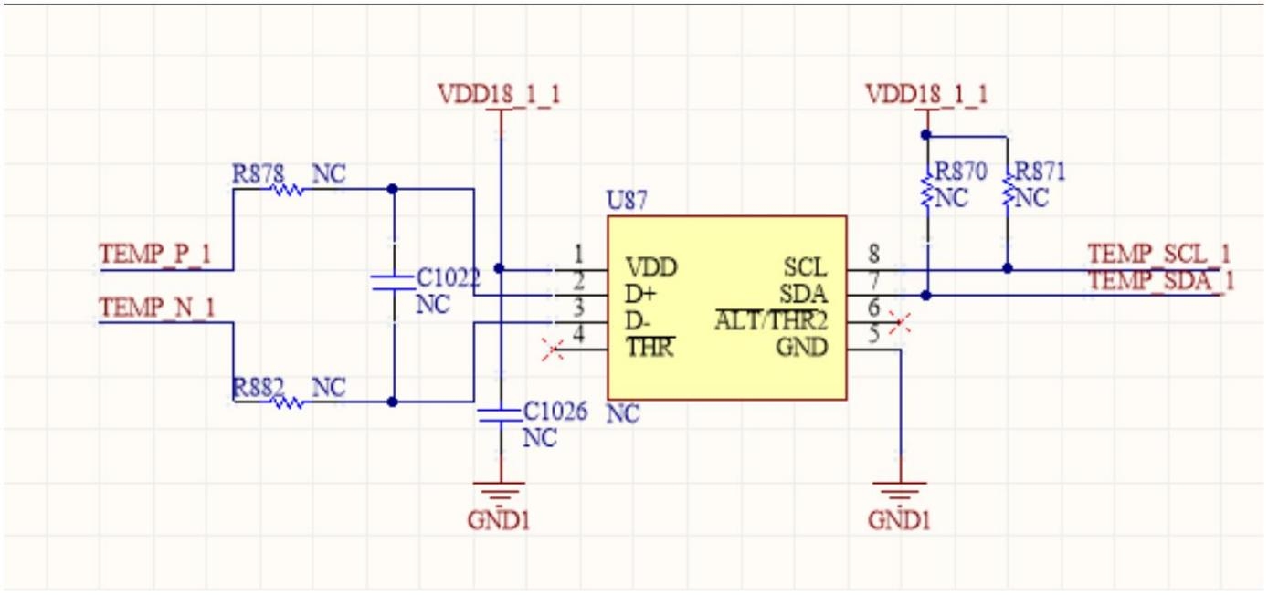
7. Temperature sensing circuit:It is composed of sensor IC. The temperature sensing chip collects the built-in temperature sensor of BM1760 through pin 6.7 of BM1760. After the temperature sensing parameters are collected, it finally passes through pins 15 and 16 of BM1760 and returns to the FPGA of the control board from RI. The principle is shown in Figure 21:
 IV. Routine maintenance process
● Reference steps:
IV. Routine maintenance process
● Reference steps:
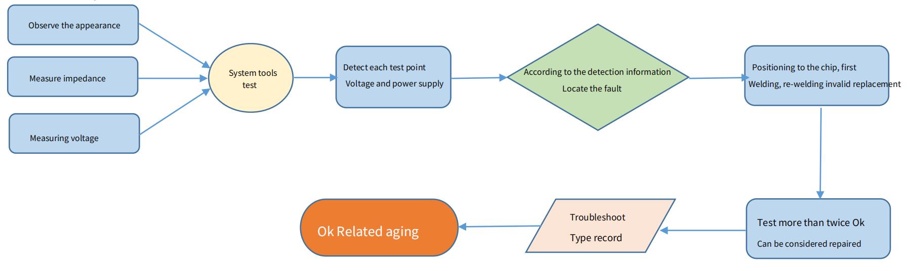
1. Routine inspection: first, visually inspect the abacus to be repaired, observe whether the small heat sink is displaced, deformed, burnt, etc., if any, must be dealt with first; if the small heat sink is displaced, first remove the loose heat sink. After disassembly, wash off the original glue, clean it, and reattach it with a thermosetting adhesive.
Secondly, after there is no problem with the visual inspection, you can test the impedance of each voltage domain first to detect whether there is a short circuit or an open circuit. If found, it must be dealt with first.
Check again whether the voltage of each voltage domain has reached 0.8V, and the voltage difference of each voltage domain must not exceed 0.05V. If the voltage of a specific voltage domain is too high or too low, the circuits of adjacent voltage domains will generally have abnormal phenomena. We need to investigate the reason first.
2. After the conventional test is no problem (Generally, the short-circuit test of the conventional test is necessary, so as not to burn the chip or other materials), check the chip with test fixture, judge, and pinpoint based on such result.
3. According to the test result displayed by the test fixture, check the chip test points (CLK IN OUT/TX IN OUT/RX IN OUT/B IN OUT/RST IN-OUT) and voltages such as VDD, VDD0V8, and VDD1V8 from the vicinity of the faulty chip.
4. Then, according to the signal flow, in addition to the RX signal being inverted (60 to 1 chip), several signals CLKCO BO RST are forwarded (1-60), and the abnormal fault is found through the serial power supply view.
5. When locating the faulty chip, the chip needs to be welded again. The method is to add flux around the chip (preferably no-clean flux), heat the solder joints of the chip pins to a dissolved state, and then gently move down and left to press the chip; to promote the re-fusion of the chip pins and the pads, and the tin is collected. To achieve the effect of tinning again.
If the fault remains the same after re-soldering, you can directly replace the chip.
6. After repairing the hash board, the test box must be inspected twice or more. Two test times before and after: the first time, after the replacement of parts is completed, the hash board needs to be cooled down, and then pass the test after passing, put it aside. For the second time, after a few minutes, wait for the hash board to cool down, test again. Although the time for the two tests is a few minutes, this does not affect the work. Put the repaired hash board aside, continue to repair the second board, wait for the second board to be repaired and set aside to cool down, and then test the first board. In this way, the time is just staggered, and the total time is not delayed.
7. It is necessary to classify the repaired hash board failure and record the replacement part's type, location, reason, etc. Be prepared for feedback from production, after-sales, and R&D.
8. After recording, install it into the whole miner for formal aging.
V. Type of failureWhen the impedance of some voltage domains deviates from the normal value, indicating that there are open and short circuits in the abnormal voltage domain. The general chip bug most likely causes it. However, there are three chips in each voltage domain, and when it fails, only one has a problem. The method to find out the problem chip can detect and compare abnormal points through the impedance of each chip's test point to the ground.
If you encounter a short-circuit phenomenon, you can first remove the heat sink on the chip with the same voltage and then observe whether the chip pins are connected to the solder.
If the short-circuit point cannot be found in the appearance, the short-circuit point can be found according to the resistance method or the current interception method.
2. Voltage unbalance in voltage domain;When the voltage of some voltage domains is too high or too low, it is generally due to abnormal voltage domains or adjacent voltage domains IO The abnormal signal condition leads to the abnormal working state of the following or next voltage domain and the voltage imbalance. Only by detecting the signal and voltage of each test point, the abnormal point can be found. Individually, it is necessary to find out the abnormal point by comparing the impedance of each test point.
Pay special attention, CLK Signal and RST Signal. These two abnormalities are most likely to cause voltage imbalance.
3. Lack of chips;The lack of a chip means that the test box cannot detect all of them during the test. For each chip, it is often impossible to detect as many chips as they are. And the actual missing (undetectable) abnormal chip is not there display. At this time, it is necessary to locate the abnormal chip through testing accurately.
The positioning method can be used TX Cut off the distribution method and find the abnormal chip's location. To convert a particular chip TX Signal to ground, connect the first 50 chip TX. After outputting the ground of the voltage domain, in theory, if all the chips in front are usual, the test fixture should display the detection 50 Chips? If not detected 50 chips, indicating that the abnormality is in the 50 chip before; if detected 50 chips, the abnormal chip is in the 50 After a chip. By analogy, use dichotomy to find the location of the abnormal chip.
4. Broken link;A broken link is similar to a lack of a chip, but a broken link does not mean that all chips that cannot find are abnormal, but because a specific chip is abnormal, all chips behind the abnormal chip fail. For example, a chip itself can work, but it will not forward other chip information; at this time, the entire signal chain will abruptly stop here, losing a large part of it as a broken link.
Generally, the broken link can be displayed in the test fixture. For example, when the test fixture detects the chip, it only detects 14. If the preset number of chips is not detected in the test fixture, it will not run, only displaying how many chips are detected. At this time, just according to the displayed number "14", In the 14, check the voltage and impedance of each test point before and after each chip to find the problem.
5. Does not run;Not running means that the test fixture cannot detect the chip information of the hash board, and it displays NO hash board; This phenomenon is the most common and involves a wide range of faults.
1) Non-operation caused by abnormal voltage in a specific voltage domain; The problem can be found by measuring the voltage of each voltage domain.
2) Caused by a chip abnormality. The abnormality can be found by measuring the signal of each test point.
CLK signal: 0.9V; The signal is output from chip 1 to 60, but the current version has only one crystal oscillator. Therefore, as long as there is an abnormal CLK signal, all subsequent signals will be searched and transmitted directly to the abnormal signal. TX signal: 1.8V; this signal is transmitted by chips 1, 2, 3,,,, 60. When an abnormality occurs at a certain point of the dichotomy, it can be detected forward.
RX signal: 1.8V; this signal is transmitted from 60, 59, 58,,,, 1. If it returns a number, please confirm the cause of the failure through the chip signal trend. For example, if the S7 and S9 hash boards are not running, the signal has the highest priority, and the signal is searched first.
BO signal: 0V, The letter No. is detected on the chip RI. When the return signal is normal, it can be pulled high. Otherwise, it is low.
RST signal: 1.8V; after power on and plugging in the hash board IO signal, the signal will change from the transmission direction of 01, 02,,,,,,60 to the last chip.
3 ) A certain chip VDD caused.
It can be measured whether the potential difference of each voltage domain is normal. In general, when the VDD voltage is 0.8V. The normal voltage of each test point in other voltage domains is also 0.8V to ensure that each electricity balances between pressure domains.
4 ) Of a certain chip VDD1V8 abnormal voltage.
Determine a certain value by measuring the test points of each voltage VDD1V8 whether the voltage is normal. Under normal circumstances, IO voltage determines the voltage of each test point, when IO voltage is 1.8V, the test points in other voltage domains are also 1.8V.
5. Low hash rate;
Low hash rate can be divided into:
1) When the test fixture is tested, the fixture receives Nonce Insufficient, which is displayed as NG. This phenomenon can be seen directly through the serial port print information of the test fixture to see the returned judgment quantity of each chip nonce. Generally, if the number of chips is lower than the set value, the excluded chip can be replaced directly, except for welding and peripheral reasons.
2) When testing the fixture, the hash rate is lower after installing the entire miner. This situation is mainly related to the heat dissipation conditions of the chip, and special attention needs to be paid to the glue used for the small heat sink of each chip and the ventilation performance of the whole miner. Another reason is that the voltage of some chips is critical. After the entire miner is installed, the difference between the 12V power supply and the power supply during the test causes a deviation between the test hash rate and the running hash rate. You can use the test box to test after turning down the test fixture and adjust the voltage to a DC adjustable power supply of 12V. After outputting, test again to find out the random number returned. This is because the chip checks the minimum number of voltage domains.
6. A chip NG ;
Refers to the test fixture serial port information showing the return of a specific chip when it passes the test fixture test nonce Insufficient or zero, the chip can be directly replaced in addition to eliminating the problem of virtual soldering and peripheral components.
● Maintenance instructions:1. During maintenance, the maintenance personnel must be familiar with each test point's function and flow direction, the normal voltage value, and the ground impedance value.
2. Must be familiar with chip soldering not to cause PCB blistering and deformation or pin damage.
3. BM1760 chip package, 14 pins on both sides of the chip. The polarity and coordinates must be aligned during welding, and they must not be misaligned.
4. When replacing the chip, the thermally conductive fixing glue around the chip must be cleaned to prevent the IC from hanging in the air or poor heat dissipation during soldering, which may cause secondary damage to the chip.
Dear Customers,
Hello, May 1-5, 2026 (GMT+8) is China's May Day, and international logistics will be suspended. Our company will suspend shipments on the afternoon of April 30, 2026, and resume warehouse shipments on May 6 (GMT+8). We are deeply sorry for the inconvenience caused to you. Thank you for your trust and support.
Best wishes,
ZEUS MINING CO., LTD.