


Antminer S21 XP Hydro H6HB7051 Repair Guide
I. Requirements for Repair Platform/Tools/Equipment Preparation
1. Platform Requirements:
Anti-static repair workbench (workbench must be grounded), anti-static wrist strap and grounding.
2. Equipment Requirements:
Constant temperature soldering iron (350℃-380℃), pointed soldering iron tip for soldering small surface mount resistors and capacitors; hot air gun temperature 350±10℃; multimeter with added soldering needles and heat shrink tubing for easy measurement (Fluke recommended); oscilloscope (Agilent recommended), network cable (requirements: connected to the Internet, stable network).
3. Repair and Testing Tool Requirements:
1) APW11 power supply, SWWEP testing must use an APW111721 power supply calibrated for power, which requires a separate material request (non-standard power supply), power adapter cable
DIY production: Use thick copper wires to connect the power supply and the hash board, 4AWG copper wire within 60cm in length is recommended for powering the hash board (production testing uses a copper bar locking method); use 19 series general-purpose test fixture, fixture base package B047 version (part number: ZJ0001000004)
2) PT1 testing supports APW9, APW9+, and APW11 power supplies
4. Repair Auxiliary Materials/Tools Requirements:
Solder paste M705, flux, PCB cleaning solution with anhydrous alcohol; PCB cleaning solution is used to clean flux residue after repair; thermal conductive gel (specification: Fujipoly SPG-30B) is used to apply to the chip surface after repair; ball grid array stencil (8mm x 8mm chip size), desoldering wick; when replacing a new chip, the chip pins need to be tinned before soldering to the hash board, and thermal conductive gel should be evenly applied to the chip surface before locking the water-cooled heat sink.
1) Barcode scanner
2) RS232/TTL adapter board, 3.3V
3) Self-made short-circuit probe (using a thumbtack for wiring and soldering)
5. Common repair spare parts requirements:
SMD resistor, 33 OHM, 1%, 1/20W, R0201 (0603), SMD resistor RES, 10K, +/-1%, 1/16W, 0402, SMD resistor Res 0 Ohm, 1/16W 0402 5%, SMD ceramic capacitor Cap, 1uF, +/-10%, 16V, X5R, 0402, SMD ceramic capacitor, 1UF, 6.3V, 20%, X5R, C0201 (0603), SMD ceramic capacitor Cap, 22uF, +/-20%, 6.3V, X5R, 0603.
II. Repair Requirements
1. Pay attention to proper handling techniques when replacing chips. The PCB board should not show any significant deformation after replacing any components. Check for missing parts, open circuits, or short circuits in the replaced components and surrounding areas.
2. Repair personnel must possess a certain level of electronic knowledge, at least one year of repair experience, and be proficient in BGA/QFN/LGA packaging soldering techniques.
3. After repair, the hash board must be tested at least twice and pass both tests before being considered acceptable. Each work order has a corresponding number of hash board SNs; each board's SN must be unique and cannot be reused during testing and scanning.
4. Check that tools and fixtures are working correctly, and verify the test software parameters and test fixture versions at the repair station.
5. For testing after chip replacement, the chip must be tested first. After passing the chip test, perform a functional test. The functional test must ensure that the water cooling plate assembly is OK. When installing the water cooling plate, the chip surface must be evenly coated with thermal conductive gel, and the cooling fan must be running at full speed or connected to a water cooling radiator and heat exchanger. When using a heat exchanger for cooling, a water pump must be added to the inlet to increase the water flow rate (used for factory PT1 testing; after-sales service can refer to using a heat exchanger).
Note: Testing PT1 without a heat sink on a single board will cause the chip to overheat and burn the board.
6. When measuring signals during PT1 chip testing, the heat sink must be locked in place; otherwise, it will cause the board to burn. PT3 testing requires connecting a heat exchanger with a water flow rate of 2-3 L/min. The water temperature must be between 32-35℃; testing cannot be performed if the water temperature is below or above this range.
7. When measuring signals and voltages with the heat sink attached, measurements can be taken on the BOT side. The bottom bracket has pre-drilled holes to facilitate measuring signal and voltage points.
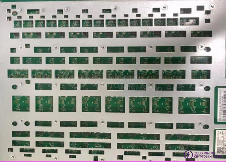
8. When replacing a new chip, the pins and solder paste must be printed to ensure the chip is pre-tinned before being soldered onto the PCBA for repair.
9. The fixtures at the repair station all use Test_Mode and barcode scanning mode for testing. After the test passes, the production line proceeds from the first test station for normal assembly and aging (according to the same level of assembly). The test configuration file can be obtained from the TE team.
10. After a PCBA with a removed heatsink is repaired successfully, the water cooling heatsink must be re-applied with thermal paste before installation and subsequent line testing (otherwise, it will cause long-term performance issues in the entire machine).
III. Fixture Fabrication and Precautions (The fixture and its accompanying clamps should facilitate water cooling of the hash board and allow for easy signal measurement.)
1. Obtain the part number: ZJ0001000004 Test Fixture, and the corresponding firmware package for the fixture's control board.
2. For the first use, update the FPGA of the fixture's control board using the S21 XP Hyd. series test fixture SD card flashing program. After decompression, copy the files to the SD card and insert the card into the fixture's card slot; power on and wait for approximately 1 minute until the control board indicator light flashes twice three times, indicating the update is complete; (Failure to update the B047 firmware package will result in testing failure and reported defects).

3.The test SD card should be created according to requirements. For PT1 chip testing and combined PT1 & PT3 functional testing, simply decompress the compressed file to create the SD card; no configuration file modification is required. The PT1 test card is used for SMT sampling inspection and for testing defective boards during repair (repaired boards must be tested again through the PT1 test process according to the production flow; repair personnel are not allowed to skip the test process).
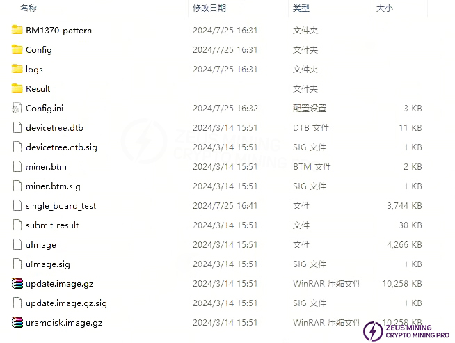
4.For production, after-sales, and outsourced repair departments, PT1 chip testing requires a barcode scanner, serial port tools, and network cables. See <<S21 XP Hyd.(H6HB7051) Single Board and Complete Machine Aging Test Procedure Guide V1.0.doc>> for details.
IV. Principle Overview
1. S21 XP Hyd. (H6HB70XXX) Hash Board Working Structure:
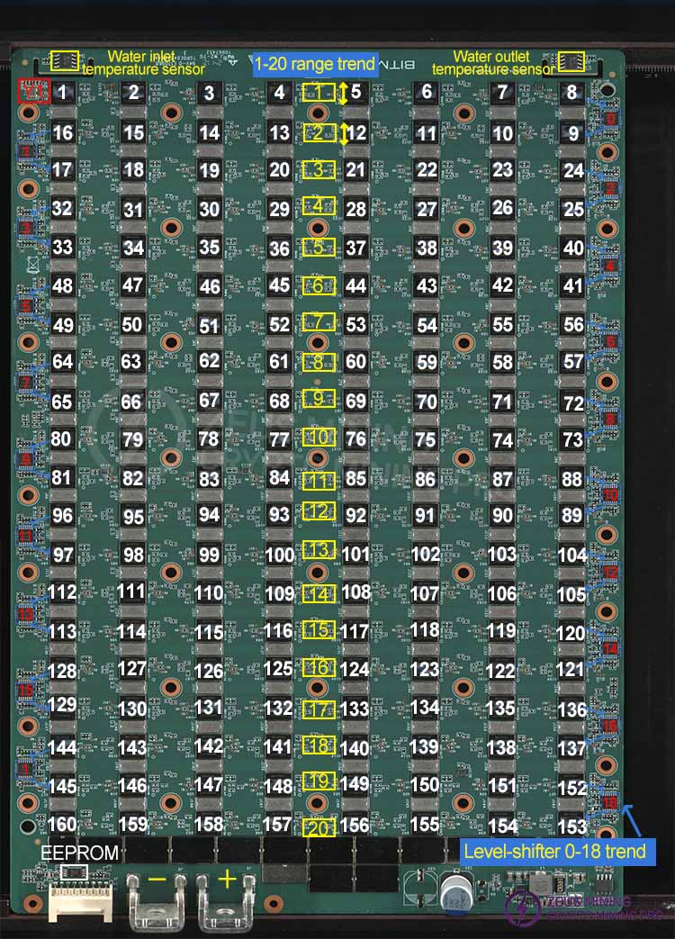
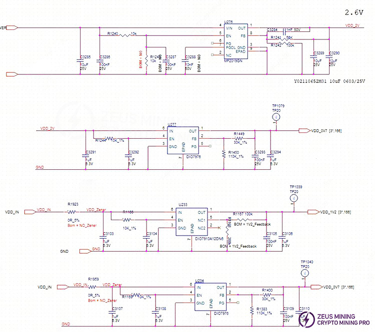
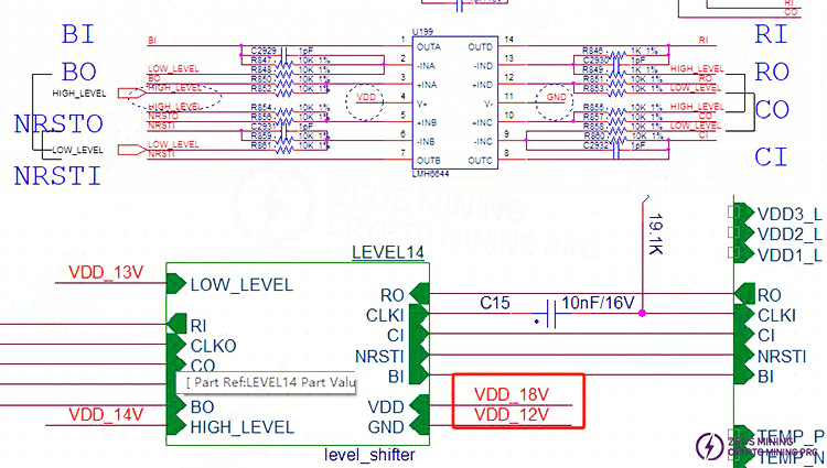
The hash board consists of 160 BM1370P chips (PCB silkscreen order BM1-BM160), divided into 20 groups (domains), each domain consisting of 8 ASICs; the BM1370P chips used in the S21 XP Hyd. hash board operate at a domain voltage of approximately 1.05V; the VDDIO of chips in domains 1-18 is powered by 1.2V & 0.7V LDOs, with each domain using 3 LDOs (one LDO outputs 1.2V, and two LDOs output 0.7V), and each 0.7V LDO supplies power to 4 chips, as shown in Figure 4-2. In the high-voltage domains 19 & 20, each domain is powered by two MP2019s (U271, U13, U276, U68) outputting 2V to the LDOs, which then supply power to the chip VDDIO. LDOs U272 & U273 (1.2V & 0.7V) are powered by U271 (MP2019), and LDOs U21 & U24 (1.2V & 0.7V) are powered by U13 (MP2019). The other two MP2019s, U275 & U68, output 2V to power two LDOs, which then output 0.7V, forming two groups as shown in Figure 4-2. Compared to other models, the S21 hash board features an LDO with a lower thermal resistance, and adds 19 level shifters to perform arithmetic operations on chip-related signals. A total of 19 level shifters are used from the second domain to the last domain, as indicated by the blue box in Figure 4-2. Level shifters 0 and 1 are powered by 6V and GND, while level shifters 2-16 are powered by 6V voltage taken across 6 domains. For example, level shifter 3 uses the voltage from the 6th domain, 7.2V-1.2VGND, and so on. Level shifters 17 and 18 are powered by the VDD_21.5V output of U147 MP2019, as shown in Figure 4-4. The temperature sensing circuit adds U98, a device that can split a single I2C bus into up to 8 independent channels, each of which can connect one or more I2C slave devices. Temperature sensing is controlled through control registers. Note that the three temperature sensors are connected to U98 via isolation ICs (NSi8100NC) for temperature control (temperature sensor U136 corresponds to isolation IC U135, U113 corresponds to U108, and U132 corresponds to U101).

The hash board has 20 domains (the chip positions in the PT3 test log are counted from 0, ASICs 0-159, and the voltage domains are also counted from 0, i.e., domain0-domain19). Note: Compared to the 1362 and 1398, the 1370P eliminates the MOS and PIC circuits and adds 19 operational amplifiers. Signal addition is performed starting from the second domain. If a defect occurs at the junction of the second domain during PT1 & PT3 testing, the operational amplifiers should be checked first. This includes checking for abnormalities in the 12M baud rate detection chip, etc. All these issues can be investigated by first checking the operational amplifiers.
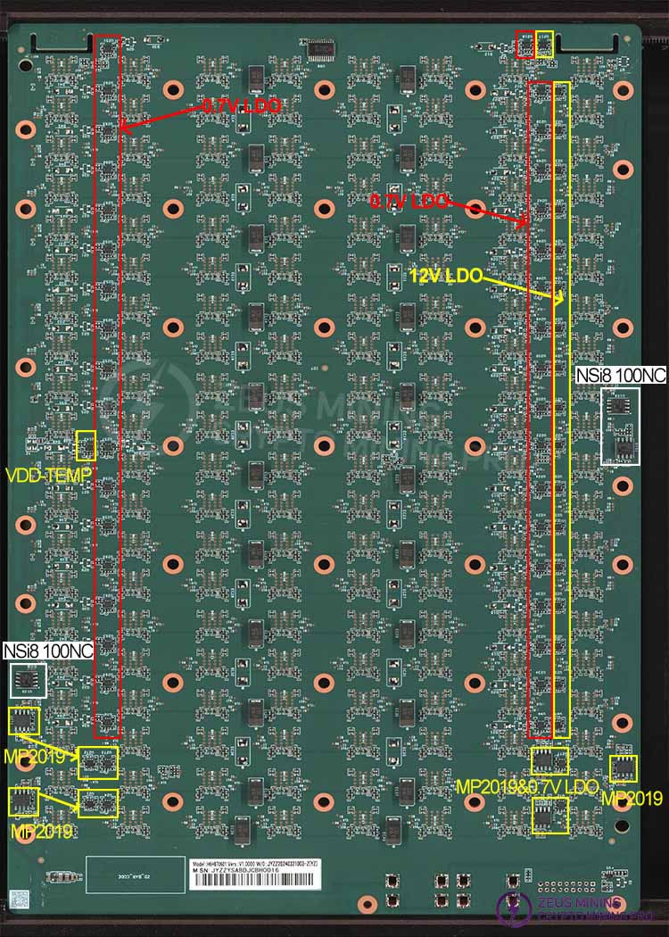
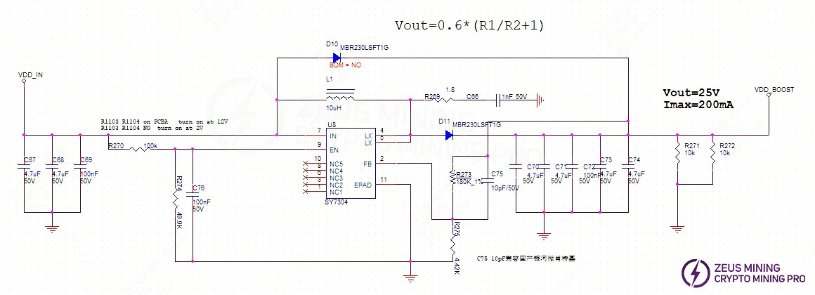
2. S21 XP Hyd. Hash Board Boost Circuit:
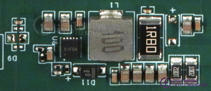
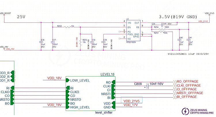
The voltage boosting is achieved by supplying power from VDD_IN through U8 to 25V, as shown in Figure 4-3.
3. S21 XP Hyd. Chip Signal Flow:
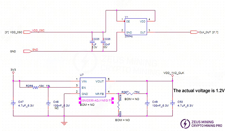
1) The CLK signal is generated by the Y1 25M crystal oscillator, and the Y1 signal is transmitted from chip BM1 to chip BM160; the voltage is approximately 0.58-0.6V.
The temperature sensor power supply is provided by U7. If there is no CLK output, first check the power supply.
4.The TX (CI, CO) signal flow is as follows: it enters from pin 7 (3.3V) of the IO port, passes through the level conversion IC U2, and then is transmitted from chip BM1 to chip BM216. The multimeter measurement shows approximately 1.1V.

5.The RX (RI, RO) signal flows from chip BM160 to chip BM1, then returns to the control board via U1 and pin 8 of the signal connector. A multimeter measurement should show approximately 1.1V.
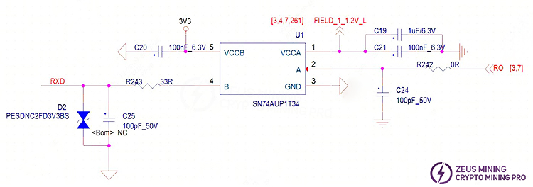
4. The BO (BI, BO) signal flows from chip BM1 to BM160;
5. The RST signal flows from pin 3 of the IO port, passes through R246, and then is transmitted from chip 01 to chip 160. The multimeter measurement shows approximately 1.2V;
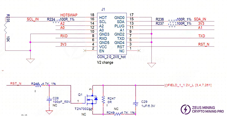
6.MP2019 & 1.2V & 0.7V LDO circuit schematic diagram (showing two sets):
7.Level shifter 0-16 circuit schematic diagram (showing one component):
8.Power supply schematic diagram for level_shifter17 and 18:
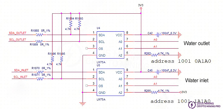
9.Schematic diagram of the inlet and outlet ports:
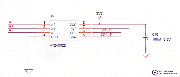
10.EEPROM schematic diagram:
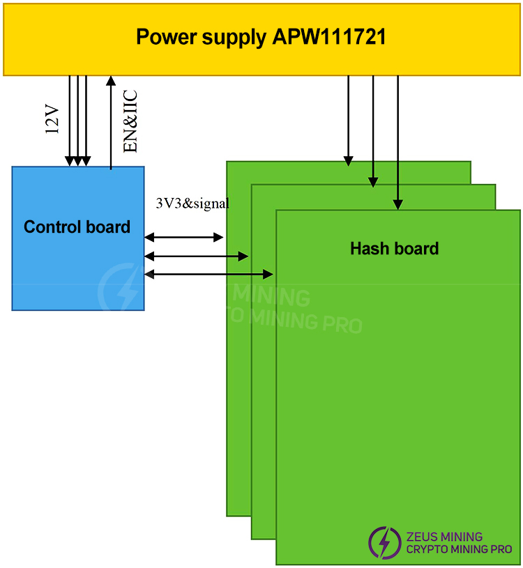
11. Overall System Architecture:
The system mainly consists of 3 hash boards, one control board, and one APW111721X power supply.
V. Common Malfunctions of the Hash Board and Troubleshooting Steps
1. Phenomenon: The single board test detects the chip as 0 (PT1 station)
Step 1: First, check the power supply output.
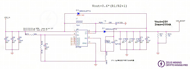
Step 2: check the voltage domain output voltage (note: measure the voltage on the bottom side with the heatsink attached; measuring without the heatsink may cause damage to the board).
Measure the voltage domain voltage to see if it is approximately 1.1V. If VDD_IN is powered, there should generally be a domain voltage. Prioritize measuring the output at the power terminals of the hash board.

Step 3: Check if CLK is being output. Measure before and after BM1. If there is an output, then measure the last component to see if it has a CLK signal. If not, use the bisection method for troubleshooting.

Step 4: Check if the LDO 1.2V and 0.7V outputs of each group are normal.
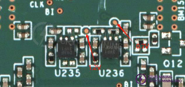
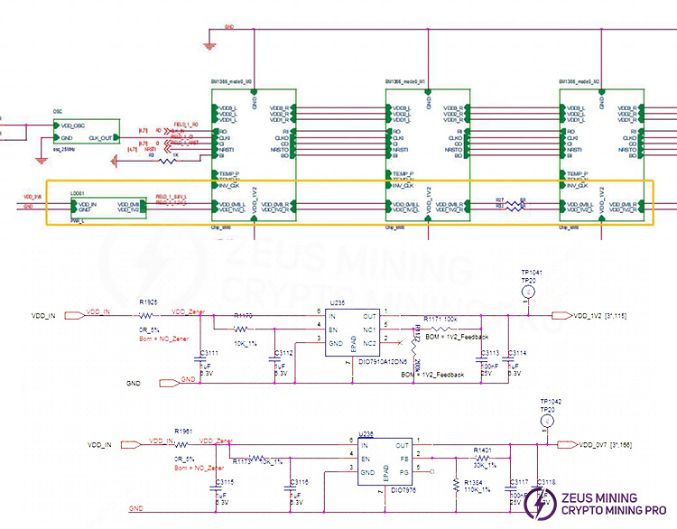
Step 5: Check the chip signal output (CLK/CI/RI/BO/RST).
Refer to the voltage range described in the signal flow diagram. If you encounter significant voltage deviations during measurement, compare the values with those of adjacent groups to make a determination.
2. If the fixture's LCD screen displays "EEPROM NG," check if U6 is soldered correctly;
3. If the fixture's LCD screen displays "sensor NG," indicating an abnormal temperature reading, troubleshoot using the following steps:
1) Check the serial port log. If sensor=0, check if the U4 and U5 chips or the adjacent surface-mount resistors and capacitors are soldered correctly;
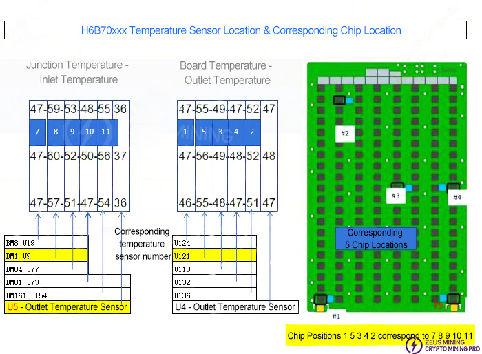
2) Sensor={0, 1}; the corresponding sensor locations are {U4, U5}; refer to Figure 4-1 for the corresponding locations. Prioritize checking if the 3.3V power supply is normal, which is output from the control board to J1.
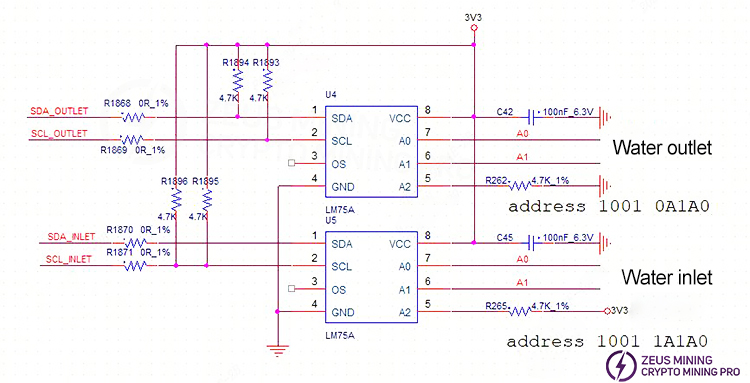
4. When the fixture's LCD screen displays "INIT NG WATER_TEMP," and the test shows abnormal water temperature readings at the inlet and outlet, check if U4, U5, and the surface-mount resistors and capacitors are properly soldered.
5. Phenomenon: Incomplete chip detection on the single board (PT1/PT3 (sweep) station)
1) When the LCD displays "ASIC NG: (0)," first measure the total domain voltage (21V) and the individual domain voltages to ensure they are normal. Then, use a shorting probe to short the RO test point and the 1V2 test point between the first and second chips, and then run the chip detection program. Check the serial port log. If it still detects 0 chips, it could be one of the following situations:
a) Use a multimeter to measure the voltage at the 1V2 and 0V8 test points to see if they are 1.2V and 0.7V. If not, there may be an abnormality in the 1.2V and 0.7V LDO circuits of that domain, or the two ASIC chips in that domain are not properly soldered. Most often, this is caused by a short circuit in the 0.7V and 1.2V surface-mount filter capacitors (measure the resistance of the relevant surface-mount filter capacitors on both sides of the PCBA), or measure whether the impedance of the chip's VDDIO to ground is abnormal. If it is abnormal, the VDDIO 1.2&0.7V resistors can be disconnected (two chips per group). If the impedance or diode value is still abnormal after disconnecting the resistors, the corresponding chip can be removed.
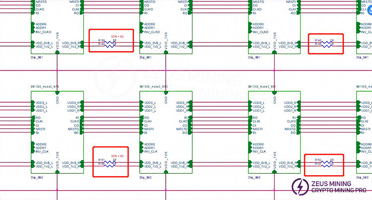
b) Check if the U1 & U2 circuits are abnormal, such as poor soldering of resistors.
c) After 1V2 and 0V8 are normal, measure the RO, RST, CLK, CI, and BI signals in sequence to check if they are normal;
d) Abnormal water temperature or heat dissipation can cause U4 and U5 to burn out, resulting in no output from the first domain's 1.2V and 0.7V, and burning out of BM1 and BM2 chips; (U4 and U5 burned out)
2) If one chip is found in step 1), it means that the first chip and the preceding circuits are good. Use a similar method to troubleshoot the subsequent chips. For example, short-circuit the 1V2 test point and the RO test point between the 38th and 39th chips. If the log shows 38 chips found, then the first 38 chips are fine; if still 0 chips are found, first check if the 1V2 is normal. If it is normal, then the chips after the 38th chip are problematic. Continue troubleshooting using the binary search method until the problematic chip is found. Assume the Nth chip is problematic. When short-circuiting the 1V2 and RO between the N-1th and Nth chips, N-1 chips will be found, but when short-circuiting the 1V2 and RO between the Nth and N+1th chips, not all chips will be found.
3) LCD displays ASIC NG: (X, a specific chip is reported) There are two cases:
a) First case: The test time is basically the same as that of a working board (usually the value of X does not change each time) (test time refers to the time from pressing the start test button to the LCD displaying ASIC NG: (X)). This is likely due to abnormal soldering of the CLK, CI, and BO series resistors before and after the Xth chip, so focus on checking these six resistors. Less likely, it is due to abnormal soldering of the following pins on one of the X-1, X, and X+1 chips;
b) Second case: The chip appearance is normal, the voltage signal is normal, but it is a problem with the chip itself;
7. Phenomenon: Multiple chips are bad, i.e., the nonce rate is slightly low (PT3 station).
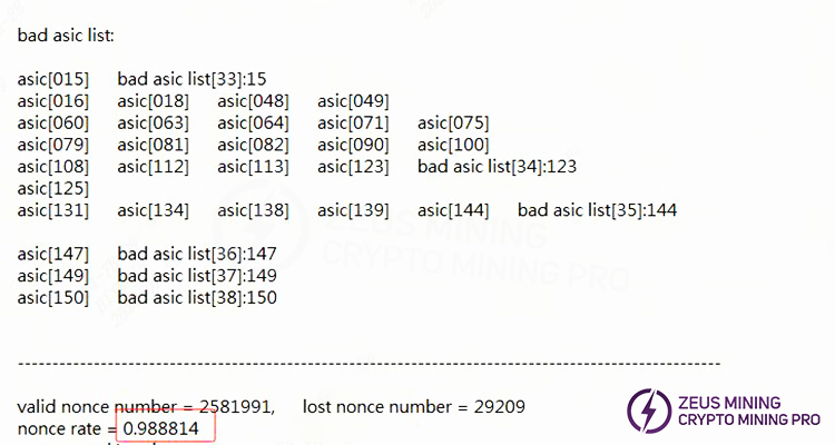
1) When encountering this situation, first check the water flow to confirm whether the test water flow is within the required range. The water temperature and flow rate of the S21 XP Hyd. directly affect the test results;
2) If the water flow is normal, check whether the copper bar voltage is within the standard range and whether there is a voltage difference;
3) After troubleshooting process-related factors, proceed to troubleshoot the heat dissipation system, specifically the water-cooled heat sink.
8. If 1 or 2-3 patterns are NG (Not Good), it indicates incomplete nonce data (PT3 station).

1) Check each individual heat sink for abnormalities; visually inspect the chip surface for foreign objects or die damage. If any are found, simply replace the affected chip;
2) Check for solder bridging or poor solder joints on the chip (a domain with two chips showing a NO CE response of 0 or 1);
3) The domain voltage is low (1.2V & 0.7V voltages are normal), indicating a defective chip;
4) Multiple chips or the entire domain show abnormal NO CE responses. Measure the domain voltage and troubleshoot the domain with the lowest voltage.
PS: Please note that both the domain and ASIC numbers start from 0; residual solder flux on the chip surface can also cause incomplete nonce responses (it is essential to thoroughly clean any residual solder flux from the surface when repairing or replacing chips).
9. Phenomenon: Chip testing is OK, but PT3 functional testing shows erratic results.
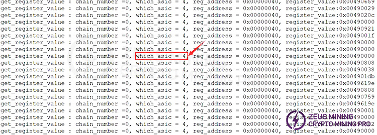
Repair method: During PT3 testing, check the serial port log. This is usually caused by an incorrect register address in a specific chip. Replace the BM5 chip (ASIC numbering starts from 0. This type of defect has not yet appeared in the pilot production. If it occurs in mass production and the defective location cannot be identified, please contact engineering for a dedicated repair program to address address errors or -1 erroneous reports).
10. Phenomenon: The first 6 domain nonces of PT3 return 0.
Repair method: Check the appearance and measure whether the signal impedance of the 6 domain chips is abnormal. This is usually caused by a short circuit in the chip or foreign matter.

11. Phenomenon: During PT3 frequency sweeping, the chip reads 0 after frequency increase.
Repair method: Check the appearance. During trial production, it was found that this is usually caused by a short circuit in the chip, solder bridging between resistors around the chip, component damage, or foreign objects.
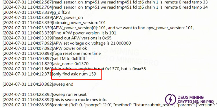
12. System Test R:1 Failure log indicates "find x asic" (where x is less than 216), meaning that not all chips on the hash board were found. Initially, if the PT1 test shows a chip abnormality, repair it accordingly. Chain0 represents board 1, Chain2 represents hash board 3, the hash board next to the power supply is board 3 (Chain2), and the middle one is Chain1 (board 2). Note that if none of the chips on all three hash boards are found, troubleshoot the power supply, voltage regulation lines, and control board.
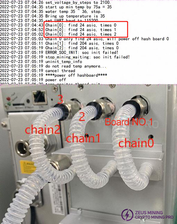
13. System-level testing JX: 1. Single chip failure, or multiple chip failures. Generally, the cooling system should be checked first. During trial production, it was also found that foreign objects under the chip caused solder bridging. After completing the process troubleshooting, replace the corresponding chip.

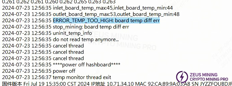
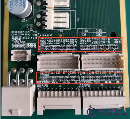
14. If the entire machine fails to start, repairs can be performed based on the log messages. Generally, cross-validation is performed first to determine whether the problem lies with the hash board, power supply, or control board. Once the scope is determined, targeted repairs can be performed. If the log shows the following errors, it is usually due to a faulty cable or a damaged component near J1. Locate the corresponding chain and troubleshoot. If everything is normal, the EEPROM information may be lost, and a retest of the PT should be performed.

15. No hash rate; caused by excessive temperature difference. Troubleshoot cooling and other related issues accordingly.
VI. Control Board Issues Leading to the Following Problems:
1. The entire machine does not operate.
1) Check if the voltage at several voltage output points is normal. If the 3.3V is short-circuited, you can first disconnect U8. If it is still short-circuited, you can remove the CPU and then measure the voltage. For other abnormal voltages, generally replace the corresponding voltage regulator IC.
2) If the voltage is normal, please check the soldering condition of the DDR/CPU (X-RAY inspection at the production end).
3) Try updating the flash program using an SD card;
For machines that use an SD card to flash the control board, the following two steps are required for normal startup:
a) After the card flashing is successful, the green LED indicator light will be constantly on. At this time, power off and restart;
b) After powering on again, wait for 30 seconds (the time required for OTP activation).
c) OTP (One Time Programmable) is a type of memory in the MCU, meaning it is one-time programmable: after the program is burned into the IC, it cannot be changed or erased again;
Precautions:
1) If the power is suddenly cut off during the OTP activation process or the time is less than 30 seconds, it will cause the control board's OTP function to fail, resulting in the control board not starting (not connecting to the network). U1 (control board main control IC FBGA) needs to be replaced. The replaced U1 cannot be used on the 19 series;
2) For control boards with the OTP function activated, U1 cannot be used on other series of models;

2. The entire machine cannot find the IP address.
This is most likely due to abnormal operation. Refer to point 1 for troubleshooting.
Check the appearance and soldering of the network port, network transformer T1, and CPU.
3. The entire machine cannot be upgraded.
Check the appearance and soldering of the network port, network transformer T1, and CPU.
4. The entire machine fails to read the hash board or has missing chains, reporting J:1.
1) Check the ribbon cable connection status.
2) Check the components of the corresponding chain on the control board.
3) Check the wave soldering quality of the connector pins and the resistors around the connector interface.
VII. System-Level Fault Phenomena
1. Initial System Testing
Refer to the test procedure document. Problems generally arise from assembly process issues or control board manufacturing issues.
Common phenomena: IP address not detected, chain detection abnormal. If an abnormality occurs during testing, repair according to the monitoring interface and test log prompts. The repair methods for initial system testing and aging testing are the same; repair according to the corresponding test item and abnormality.
1) Phenomenon: P:1 (Prioritize checking if the water inlet temperature is too high and if the water flow rate is normal. Generally, this is due to the temperature exceeding the standard, triggering over-temperature protection. If a specific chip shows over-temperature protection, after checking the water temperature and flow rate, check for abnormalities in the cooling of the hash board according to Figure 4-1.)
2) Phenomenon: JX:1 (Chip bad ASIC. Prioritize checking the cooling system. If the cooling system is normal, it is generally due to a defective chip.)
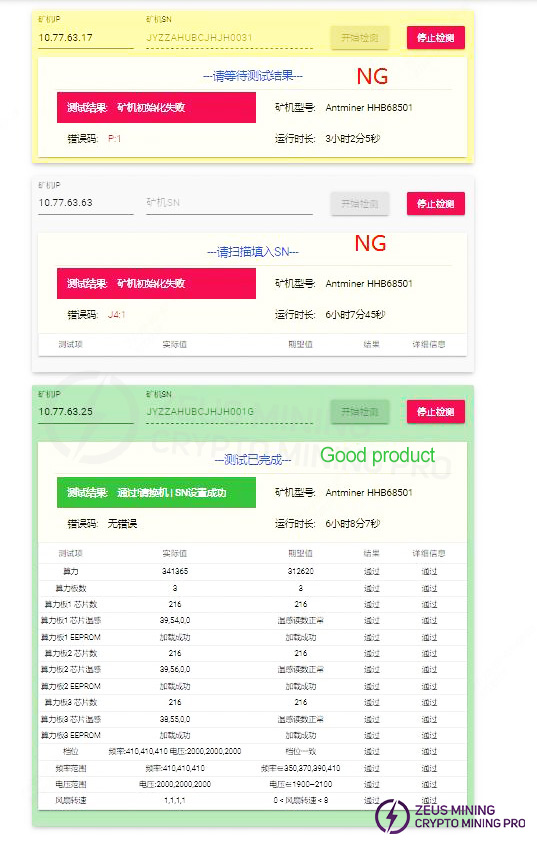
2. Aging Test: During the aging test, repairs should be performed based on the monitored interface test, for example:
1) Missing Chain: A missing chain means one of the three boards is missing. In most cases, this indicates a problem with the connection between the hash board and the control board. Check the ribbon cable for any open circuits. If the connection is OK, perform a PT3 test on the single board to see if it passes. If it passes, it can basically be determined that the problem is with the control board. If it fails, use the PT3 repair method for repair.
2) Abnormal Temperature: Generally, this refers to high temperature. Our monitoring system sets the maximum PCB temperature at 80 degrees Celsius and the chip temperature at 95 degrees Celsius. If the temperature exceeds these limits, the machine will alarm and cannot work normally. Generally, you can check if the outlet water temperature exceeds 45 degrees Celsius, which can cause this problem. Thermal conductive gel can also cause abnormal temperatures.
3) Incomplete Chip Detection (OM firmware can boot and run, but IM firmware cannot; OM firmware hash rate is 2/3 or 1/3 of the normal value): Check the log to see if there are insufficient chips. If there are insufficient chips, refer to the PT1 & PT3 test and repair procedures;
4) No hash rate after running for a period of time, pool connection interrupted: Check the network;
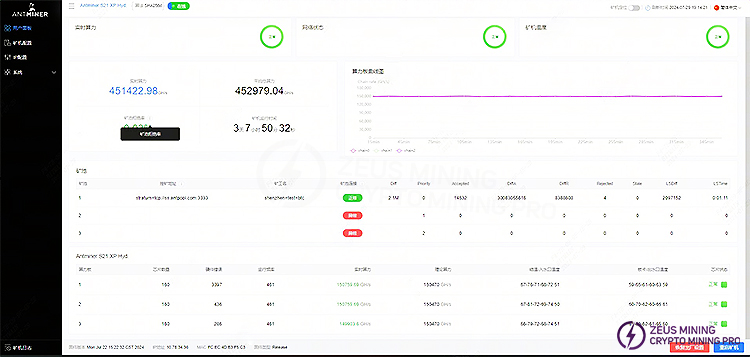
5) Aging test status of a normal, working machine.
3. After-sales service and production maintenance of water-cooled test platform setup (test water temperature: 32-35℃, single board water flow rate: 2-3 L/min)
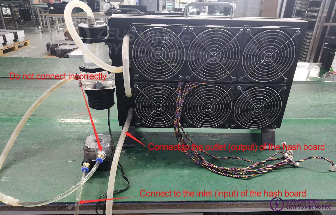

1) Because the first-generation water cooling system did not meet the requirements, the modification requires adding a water pump in series (or connecting two radiators in series), or testing on the production line test bench. Alternatively, you can purchase a radiator with better cooling performance as shown in the image below. The production team recommends testing on the water-cooled test bench, while a standard radiator can be used for PT1 testing during repairs.
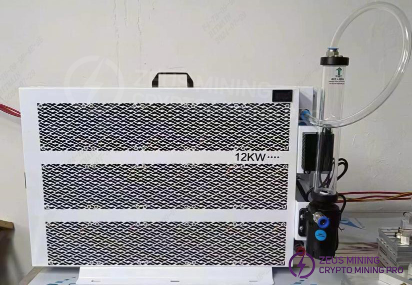
2) Use 8mm water pipe connectors during the modification; if the heat dissipation is insufficient, an air cooling fan can be added for assistance;
Refer to the troubleshooting steps for each station above. For details on the relevant testing procedures and test fixtures, please consult with the after-sales engineer. After repair, you can use the scanning mode to test PT1 and then test PT3.
VIII. Other Important Notes
Repair Process Flowchart
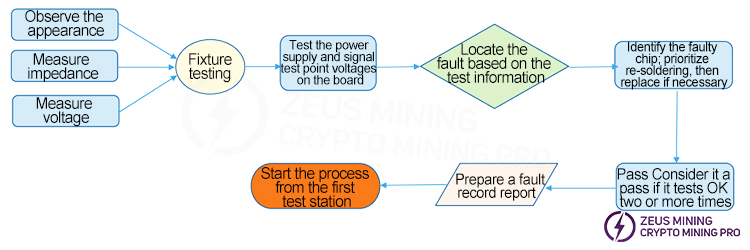
1. Routine Inspection: First, visually inspect the hash board to be repaired for any deformation or burning of the PCB. If any are found, they must be addressed first.
Check for any components with obvious burn marks, displaced or missing components due to impact, etc. Secondly, if there are no visual problems, the impedance of each voltage domain can be tested to check for short circuits or open circuits. If any are found, they must be addressed first. Thirdly, check if the voltage in each domain is approximately 1.2V.
2. After the routine inspection is complete (the short-circuit test in the routine inspection is essential to prevent damage to chips or other materials due to short circuits during power-on), a test fixture can be used to test the chips, and the results of the test fixture can be used to determine the location of the fault.
3. Based on the test results displayed by the test fixture, start from the vicinity of the faulty chip and test the chip test points (CI/RST/RO/CLK/BI) and voltages such as VDD0V8 and VDD1V2.
4. Then, according to the signal flow, except for the RO signal which is transmitted in reverse (from chip 216 to chip 1), several signals CLK, CI, BI, and RST are transmitted in the forward direction (1-216). The abnormal fault point can be found by following the power supply sequence.
5. When the faulty chip is located, the chip needs to be re-soldered. The method is to add flux around the chip (preferably no-clean flux), heat each solder joint of the chip pins to a molten state, and promote the re-bonding and tinning of the chip pins and solder pads. This achieves the effect of re-tinning. If the fault persists after re-soldering, the chip can be replaced directly.
6. After the hash board is repaired, it must pass the test fixture test at least twice to be considered a good product. The first time, after replacing the components, wait for the hasht board to cool down, and after passing the test with the test fixture, set it aside to cool further. The second time, wait a few minutes for the hash board to cool completely before testing again.
7. After the hash board is successfully repaired, relevant repair/analysis records must be made (repair report requirements: date, SN, PCB version, component location, cause of failure, responsibility for failure, etc.). This is for feedback to production, after-sales service, and R&D.
8. After recording the necessary information, the unit is reassembled for standard aging testing.
9. Repaired good units from the production line must start the process from the first production station (at least the appearance inspection and PT1/PT3 testing stations).
10. For defective hash boards that have been repaired, the thermal conductive gel on the heat sink must be reapplied (otherwise it will cause abnormal temperature differences) before they can proceed through the production line.
Dear Customers,
Hello, April 4, 5 and 6, 2026 (GMT+8) are the traditional Chinese festivals - Qingming Festival. Our company will suspend shipments during these 3 days and resume shipments on April 7 (GMT+8). We are deeply sorry for the inconvenience. Thank you for your understanding and support.
Best wishes,
ZEUS MINING CO., LTD.