


Antminer E9 Hash Board Repair Guide
I. Maintenance Platform / Tool / Equipment Preparation Requirements
1. Platform requirements:
Anti-static repair workbench (the workbench needs to be grounded), the reapirman must wear anti-static wrist straps.
2. Equipment requirements:
(1) Constant temperature soldering iron (350-380 degrees) and pointed soldering iron tip: used to solder the small patches such as patch resistors and capacitors;
(2) Hot air gun and BGA rework station: used for chip / BGA disassembly and welding;
(3) Multimeter: add the welded steel needles and put on a heat-shrinkable sleeves for easy measurement, Fluke is recommended;
(4) Oscilloscope: recommended to use Agilent;
(5) Network cable: connect to the Internet and have a stable network.
3. Test tool requirements:
(1) APW12 PSU (AP12_12V-15V_V1.2 and power adapter cable): used for power the hash board.
DIY: Use thick copper wires to connect the power supply and the hash board. It is recommended to use 4AWG copper wires with a length of less than 60cm, which are only used for PT2 and maintenance tests;
(2) Test fixture for V2.0 control board (test fixture part number: NA)
The positive and negative poles powering of the test fixture need to be equipped with a discharge resistor, and it is recommended to use a cement resistor of 20 ohms and above 100W. For easy repair, PicoBT multifunctional test fixture can also be used.
4. Maintenance auxiliary materials / tools:
(1) Solder paste M705, flux, board washing water and absolute alcohol, washing board water is used to clean up the flux residue after maintenance;
(2) Thermal gel, specification: Fujipoly SPG-30B, used to apply on the surface of the chip after maintenance;
(3) Ball planting stencil, tin suction wire, solder balls (ball diameter recommended 0.5mm): When replacing a new chip, it is necessary to plant the ball to the chip and then solder it to the hash board. Spread heat-conducting gel evenly on the surface of the chip and install it for heat dissipation device.
(4) Scanning gun
(5) Port adapter board RS232/TTL adapter board 3.3V
(6) Self-made short-circuit probe: Use pins for wiring and welding, and heat shrinkable sleeves to prevent short-circuiting between the probe and the small heat sink.
5. Common maintenance spare materials:
0402 resistors (0R, 51R, 10K, 4.7K,); 0402 capacitors (0.1uf, 1uf)
Ⅱ. Maintenance requirements
1. Pay attention to the operation method when replacing the chip. After replacing any accessories, the PCB board does not have obvious deformation. Check whether there are a few open and short circuits in the replaced parts and the surrounding areas.
2. Maintenance personnel must have certain electronic knowledge, more than one year of maintenance experience, and be proficient in BGA / QFN / LGA packaging welding technology.
3. After repairing, the hash board must be tested for more than two times and it is OK before it can pass!
4. Check whether the tools and fixtures can work normally, determine the parameters of the maintenance station test software, the version of the test fixture, etc.
5. For the test of chip repair and replacement, it is necessary to first check whether the capacitor on the back of the chip is short-circuited, and then do a functional test after passing. The functional test must ensure that the heat sink is installed in place (each thermal conductive adhesive must be applied evenly before installing the heat sink), and the cooling fan is at full speed. When using the chassis for heat dissipation, one hash board should be placed at the same time to form an air duct. The single-sided test of production should also ensure the formation of an air duct (important)
6. When measuring signals, 4 fans are used for cooling, and the fans keep at full speed.
7. When powering on the hash board, you must first connect the negative copper wire of the power supply, then the positive copper wire of the power supply, and finally insert the signal cable. When disassembling, the order of installation must be reversed, first remove the signal cable, then remove the positive copper wire of the power supply, and finally remove the negative copper wire of the power supply. If you do not follow this order, it is very easy to cause damage to U1 and U2 (the full chip cannot be found). Before testing the pattern, the repaired hash board must be cooled down before testing, otherwise it will cause PNG to be tested.
8. To replace a new chip, print pins and solder paste to ensure that the chip is pre-tinned and then soldered to the PCBA for maintenance.
9. The fixtures on the maintenance end use the Test_Mode and use the code scanning mode to test. After the test passes, the production end streamlines from the first station of the test, and the normal installation is aging (installed at the same level).
Ⅲ. Test fixture production and precautions
The supporting the test fixture should satisfy the heat dissipation of the hash board and facilitate the measurement of signals.
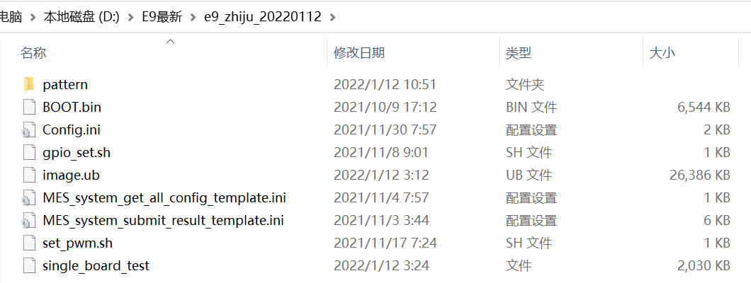
1. The E9 test file name is as follows, and the indicator lights are as follows;


2. Make the test SD card according to the requirements, just decompress the compressed package directly to make the SD card. Special attention: sometimes the software configuration Config file may not be PT2 in the original package, so be sure to confirm whether it is PT2 configuration file, plug in the network cable and the scanner when testing PT2.
Ⅳ. Principle overview
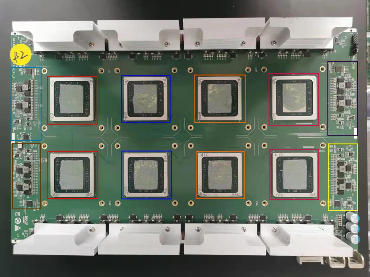
1. Working structure of E9 hash board:
The hash board is composed of 8 BM1798 chips, and every two chips share a set of power management chips.
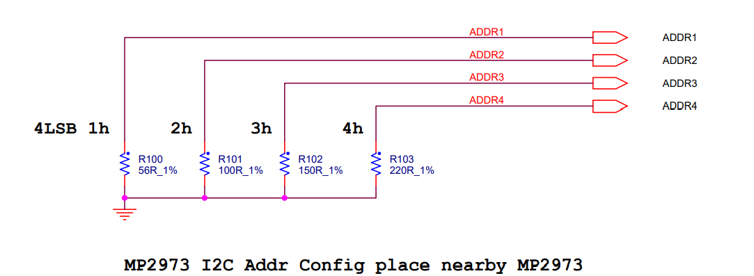

2. E9 hash board MOS voltage circuit:
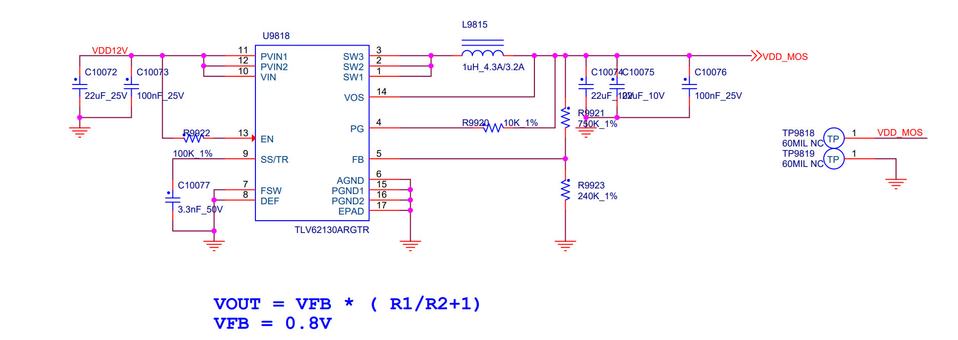
3. Signal direction:
(1) CLK (XIN) signal flow direction, four groups are generated by the U1003 crystal oscillator, and each group transmits two chips; the voltage is about 0.8V-0.9V;
(2) RST and CI signals flow direction: from pin 24 (3.3V) of the IO port, through the level conversion IC U1-U8, and then transmitted from chip 01 to chip 8; the voltage is 0V when the IO cable is not inserted, test reported 0;
(3) RX (RI, RO) signal flow direction, from No. 8 chip to No. 01 chip, and return to the signal cable terminal pin 15 through U10 and return to the control board; the voltage is 0.3V when no IO signal cable is inserted, and the voltage is 1.2V during operation;
(4) BO (BI, BO) signal flow direction, from No. 01 chip to No. 8; the multimeter measures 0V;
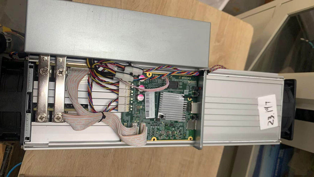
4. Machine structure:
The whole machine is mainly composed of 2 hash boards, 1 control board, 1 APW12 power supply, and 4 cooling fans, as shown:
Ⅴ. Common defects of hash board and troubleshooting steps
1. Phenomenon: the board test detection chip is 0 (PT2 station)
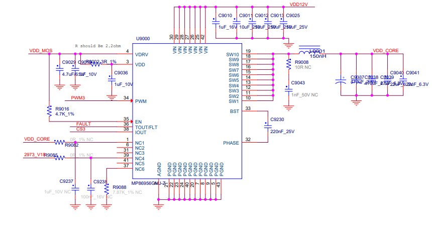
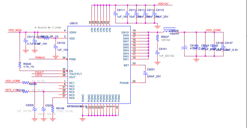
Step 1: check the power output first, please check whether all voltages of U9000-U9010 are normal;
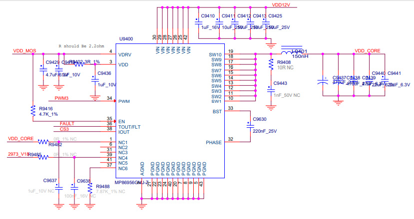
Step 2: Check the output of the voltage tube: whether the voltage of each voltage tube from U9401-U10210 is normal, continue to check down.

Step 3: check the PIC circuit: measure whether there is an output of about 3.2V on the 11th pin of U6, if there is, please continue to troubleshoot the problem; if there is no 3.3V, please check whether the connection between the fixture cable and the hash board is OK. If not, please reprogram the PIC.

How to burn PIC chip?
(1) Hash board PIC file burning:

Download the burning tool: MPS, Server Telecom Core Power Monitor Programming
(2) Burning software reference burning:
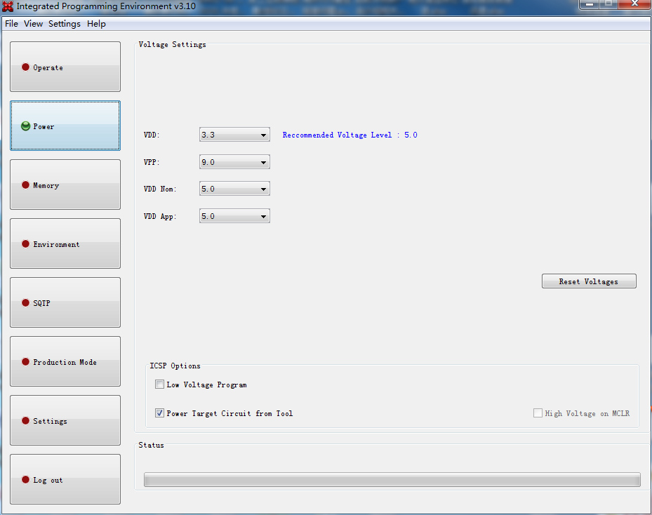
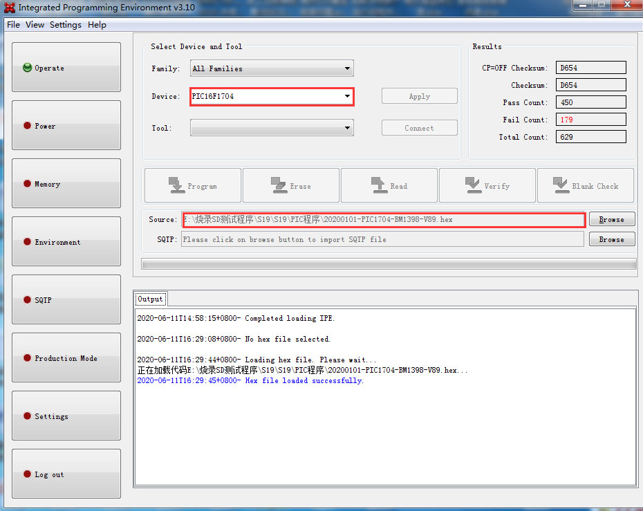
Open MPLAB IPE, select device: PIC16F1704, click power to select the powering method, and then click operate.
① Select file to find the .HEX file to be burned;
② Click "connect" to connect normally;
③ Click "program" button, and click "Verify" after completion, and it will prompt that the verification is completed to prove that the programming is successful.

(3) Measure whether the output of the power management chip is normal. If the output is abnormal and there is no process problem, it is necessary to reprogram the Core information of the power management chip. For specific programming, refer to the following documents:
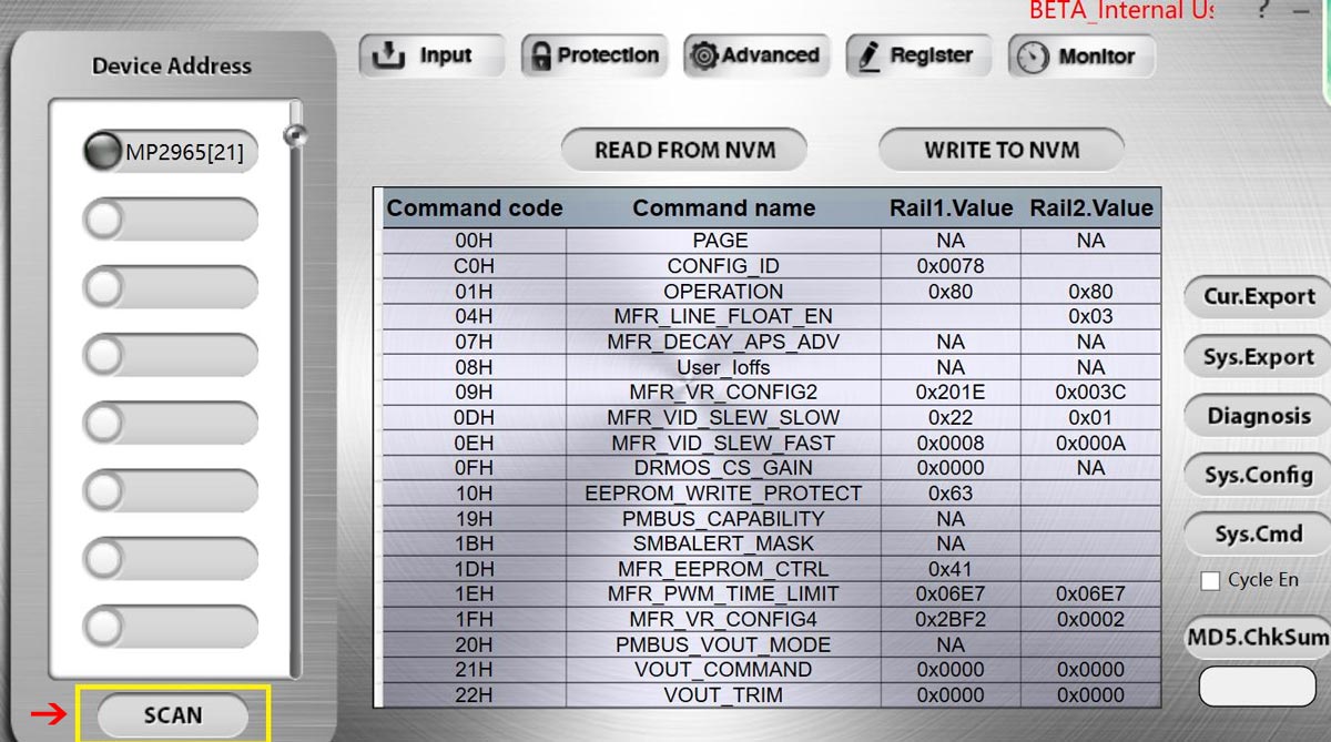
① Install the USB to I2C driver and Server GUI software;
② Click the desktop shortcut: MPS, Server Telecom Core Power Monitor Programming
③ Click SCAN to find the IC with the corresponding address (just an example, the address and part number are subject to the actual situation);
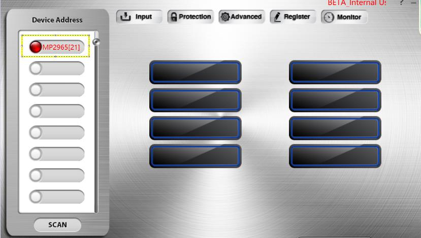
④ Select the IC with the corresponding address, it will turn red after selection as follows:
2. Phenomenon: the board Pattern NG, that is, the reply nonce data is incomplete (PT2 station)
Pattern NG is caused by the fact that the characteristics of some chips are quite different from other chips. At present, it is found that the die of the chip is damaged, so it is only necessary to replace the chip. According to the log information, the replacement rule is:
If the appearance of the chip is not damaged, just replace the chip with the lowest response rate in each domain. From the log, you can see whether the chip is normal, or command query;
PS: Special attention should be paid to the numbering of domain and ASIC chip starting from 1.
3. Phenomenon: Check the chip test is OK, but the PT2 function test serial port does not stop (long running)
Repair method: During the PT2 test, look at the serial port print log. When the serial port starts long running, use the short-circuit probe to short-circuit RO&1.8V, and start short-circuiting from the first chip. If the serial port stops long running after short-circuiting, it means that the first chip is OK, according to this method to find the chip that still fails after a short-circuit of a certain chip, usually it is caused by a certain chip, just replace it;
PT2 test environment requirements: The temperature of the PT2 test environment should be between 20°C and 30°C. When the ambient temperature exceeds 35 degrees, the software will stop the test.
PT2 test powering requirements: PT2 test fixture powering under the load of 1500 watts (in the case of testing a board), the actual output voltage cannot be lower than 0.03V set in the configuration file. (For example, if the configuration file requires trial production of 15V, then the output voltage of the powering cannot be lower than 14.97V when it is loaded with 1500 watts).
Ⅵ. Control board problems cause the following problems
1. The whole machine does not run
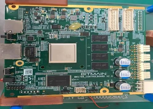
(1) Check whether the voltage of several voltage output points is normal. If there is a 3.3V short circuit, you can disconnect U33 first. If the short circuit is still present, you can unplug the CPU and measure again. If other voltages are abnormal, replace the corresponding converter IC.
(2) If the voltage is normal, please check the welding status of DDR / CPU (X-RAY inspection at the production end).
(3) Try to update the flash program with SD card.
2. The whole machine cannot find the IP
There is a high probability that the IP cannot be found due to abnormal operation. Refer to point 1 for troubleshooting. Check the appearance and welding condition of the network port, network transformer T1, and CPU.
3. The whole machine cannot be upgraded
Check the appearance and welding condition of the network port, network transformer T1, and CPU.
4. The whole machine fails to read the hash board or there are few chains
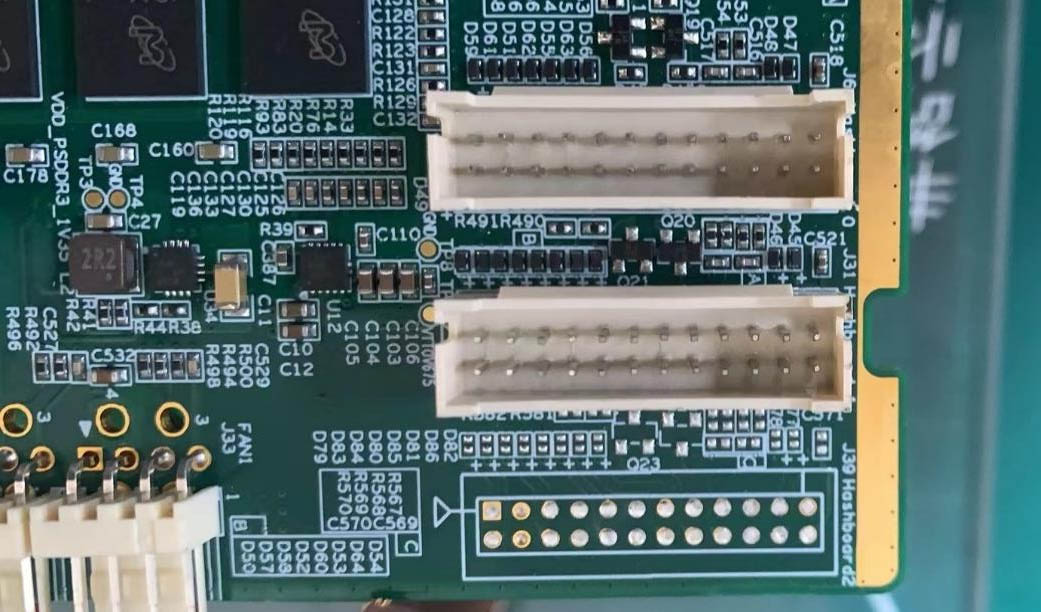
a. Check the cable connection condition.
b. Check the part of the control board corresponding to the chain.
c. Check the wave soldering quality of the row pins and the resistance around the plug-in interface.
Ⅶ. Fault phenomenon of the whole machine
1. Preliminary test of the whole machine
Referring to the test process document, the general problems are assembly process problems and control board process problems.
Common phenomena: IP is not detected, the number of fans is detected abnormally, and the chain is detected abnormally. During the test, if there is an abnormality, it should be repaired according to the monitoring interface and test LOG prompts. The maintenance methods of the initial test of the whole machine and the aging test are the same.
2. Aging test: during the aging test, maintenance should be carried out according to the monitored interface test, for example;
(1) The display of the fan is abnormal: we need to check whether the fan works normally, whether the connection with the control board is normal, and whether the control board is abnormal.
(2) Few chains: Few chains mean that 2 boards are missing 1 board. In most cases, there is a problem with the connection between the hash board and the control board. Check the cable to see if there is an open circuit. If the connection is OK, you can test the single board with PT2 to see if it can be tested. If it can be tested, you can basically confirm that it is the control board. If it fails the test, use the repair method of PT2 to repair it.
(3) Abnormal temperature: Generally, the temperature is high, the PCB temperature set by our monitoring system cannot exceed 80 degrees. If it exceeds 80 degrees, the machine will alarm and cannot work normally. It is usually caused by the high ambient temperature and the fan is working anomalies can also cause temperature anomalies.
(4) After running for a period of time, there is no hashrate, and the connection to the mining pool is interrupted. Check the network.
(5) The aging test status of the normal good product machine;
3. For the single board test OK after assembling the whole machine for testing, a hash board has no hashrate after running for about 3 minutes:
The specific analysis method is as follows;
(1) Carry out the PT2 test of the single board first to see if the board is OK. If the test chip is not complete, then repair the single board;
(2) If the normal gear position is OK after the test, then take out the board separately, use the test fixture to carry it into the master chip program of DeBug for mining, adjust the fan speed to 95%, and adjust the voltage frequency to work for the whole machine voltage and frequency, let the machine perform mining, and see if the machine loses hashrate in the end;
(3) If the machine still loses hashrate, then reduce the frequency to 200M and other conditions remain unchanged, let the machine mine to see if it will lose hashrate, whether the hash board will hit X, if it still hits X and lose hashrate, then you can remove the heat sink of the hash board for mining;
(4) When the hashrate is lost, measure whether the voltage of the domain is normal. In general, the domain with a problematic domain voltage will appear abnormal, and then measure the RI signal to see where the RI signal is broken. If the RI signal is gone, basically the chip is short-circuited or damaged after being tinned.
Ⅷ. Other matters needing attention
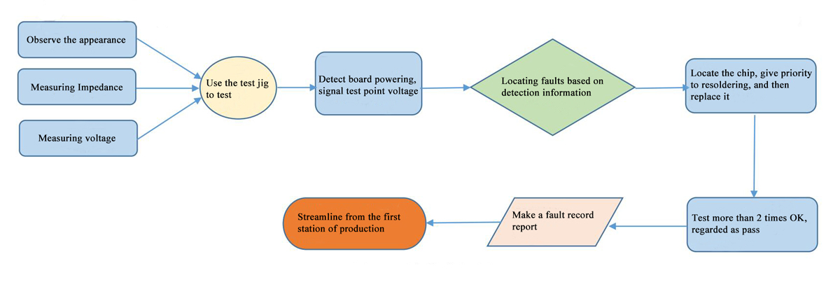
1. Routine inspection: First, visually inspect the hash board to be repaired to see if there is PCB deformation or scorching. If there is any phenomenon, it must be dealt with first; whether there are obvious signs of burnt parts, parts impact offset or missing parts, etc.; Secondly, if there is no problem with the visual inspection, the impedance of each voltage domain can be detected first to detect whether there is a short circuit or an open circuit. If found, it must be dealt with first. Third, check whether the voltage of each domain is about 0.32V.
2. After the routine inspection is ok (short circuit detection of general routine inspection is necessary, so as not to burn the chip or other materials due to short circuit when the power is turned on), the chip can be tested with the test fixture, and the judgment and positioning can be carried out according to the test result of the test fixture.
3. According to the display results of the test fixture, start from the vicinity of the faulty chip, and check the chip test points (CO/NRST/RO/XIN/BI) and voltages such as VDD0V8 and VDD1V2.
4. When the faulty chip is located, the chip needs to be unsoldered again. The method is to add flux (preferably no-clean flux) after the chip is ball-planted, and solder on the BGA rework station. If the fault is still the same after re-soldering, the chip can be replaced directly.
5. For the repaired hash board, when testing with the test fixture, it must pass more than two times before it can be judged as a good product. For the first time, after the replacement of accessories is completed, wait for the hash board to cool down, use the test fixture to test the pass, and then put it aside to cool down. The second time, wait for the hash board to cool down completely every few minutes before testing.
6. After the hash board is repaired OK. It is necessary to make relevant maintenance analysis records (maintenance report requirements: date, SN, PCB version, bit number, cause of failure, attribution of failure responsibility, etc.). In case of feedback back to production, after-sales, and research and development.
7. After the record is completed, it will be assembled into a complete machine for routine aging.
8. Good products repaired at the production end should be streamlined from the first station of production (at least the appearance inspection and PT2 test station)!
9. For defective Hashboards that have been repaired, the heat conduction gel must be removed and reprinted before the heat sink can be streamlined!
Dear Customers,
Hello, May 1-5, 2026 (GMT+8) is China's May Day, and international logistics will be suspended. Our company will suspend shipments on the afternoon of April 30, 2026, and resume warehouse shipments on May 6 (GMT+8). We are deeply sorry for the inconvenience caused to you. Thank you for your trust and support.
Best wishes,
ZEUS MINING CO., LTD.