


Antminer S19j Pro Aluminum Hash Board Repair Guide
Ⅰ. Repair platform / Tools / Equipment Preparation
1. Platform requirements
A grounded anti-static maintenance workbench is required, and maintenance personnel must wear anti-static wrist straps.
2. Equipment requirements
(1) Constant temperature soldering iron (350°C-380°C / 662°F-716°F) and pointed soldering iron for soldering SMD resistors, capacitors and other small patches.
(2) Heat guns, heating table (350°C-400°C) and BGA rework stations for chip and BGA desoldering and welding.
(3) A multimeter (Fluke is recommended) with welded steel needle and heat-shrinkable sleeve for easy measurement.
(4) Oscilloscope.
(5) Network cable (requirement: stable Internet network).
3. Test Tool Requirements
Use APW12 power supply to build a test platform (Recommended to use APW12 12V-15V V1.2 and power adapter cable):
(1) Use thick copper wires to connect the positive and negative poles of the PSU and the hash board. It is recommended to use 4AWG copper wires with a length less than 60cm (only for PT1 and maintenance tests), which can be used to power the hashboard.
(2) Use the V2.2010 control board test fixture (model ZJ0001000001), and the positive and negative poles of the power supply need to be equipped with discharge resistors. It is recommended to use 20 ohm cement resistors above 100W; or you can also use the PicoBT multi-function test jig.
4. Repair auxiliary materials and tools requirment
(1) Solder paste M705, flux, hash board cleaner, anhydrous alcohol, thermal conductivity gel, implant ball stencil (6*6 chip size), suction solder wire, tin ball (recommended diameter 0.4mm).
(2) Circuit board cleaners for cleaning flux residues after repairs;
(3) After maintenance, apply FujipolySPG-30B thermal grease on the surface of the chip;
When replacing a new chip, it is necessary to tin-plant the pins of the chip first, then solder it to the hash board, and evenly apply thermal conductive silicone grease on the surface of the chip, and finally install the large heat sink.
(4) ZD2200 Wired Scanner
(5) TTL to RS232 serial port module
(6) Self-made short-circuit probe (large-headed needle wiring is used for soldering, and it is required to heat shrink sleeve to prevent the probe and small heat sink short circuit.)
5. Common maintenance spare materials:
0402 resistors: 0R, 33R, 51R, 10K, 4.7K
0402 capacitance: 0.luF, luF
Ⅱ. Operation Requirements
1. Maintenance personnel must have certain electronic knowledge, more than one year of maintenance experience, and be proficient in BGA/OFN/LGA packaging welding technology.
2. The repaired hash board must pass two or more tests before it can be qualified.
3. When replacing the chip, pay attention to the operating specifications, ensure that the PCB board is not deformed after replacing the parts, and check whether there are missing parts, open circuit and short circuit around the replaced parts.
4. To test the replaced chip, test the chip first, and then perform the functional test (PT2). Ensure that the small heatsink soldering is OK and large thermal instalation in place (each thermal adhesive must be applied evenly after the installation of a large heatsink). and the cooling fan is at full speed. To use chassis for cooling, it is required to put 2 pieces of hashboard at the same time to form a duct, which is also required (and important) for the single-sided test of production.
5. To power on hash board, put the negative and positive copper wire in place in sequence, and finally insert the signal cable. Removal must be performed in the reverse order, ie. removing the signal cable, followed by the positive and negative copper wire of power supply Failure to follow this order may cause U1 and U2 damage (failure to find the chip in complete). Before pattern test, the repaired hash board must be cooled down before testing, otherwise it will lead to test PNG.
6. Confirm the miner needs to be repaired, the corresponding test software parameters and test fixture.
7. Check the tools and fixture whether they can work properly.
8. Fans are used for cooling purpose when measuring signals, so it is required to keep 4 fans running at full speed.
9. Replace the new chip to clean the pins and apply solder paste to ensure that the chip is coated with tin before soldering.
Ⅲ. Fixture Setup and Precautions
1. Fixture model: ZJ0001000001
2. For the first time to use S19j pro series, complete FPGA update for the fixture control board with test fixture SD card swiping program, unzip and copy to SD card, insert the memory card into fixture card slot. Power on for about 1 minute and wait for the control board indicator to double flash 3 times after the update is completed (failure to update may cause the reporting of a bad chip during test).
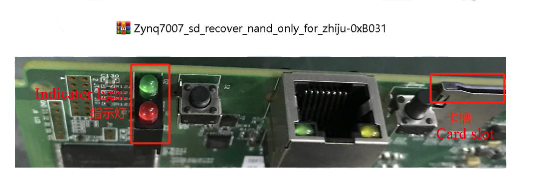
3. Setup of SD card without heat sink: repair using REPALR's program, the following screenshot ilustrates that this program does not need to scan the code. During measurements, heat dissipation is required for PCBA, in order to prevent the test, measurement process board overheating.
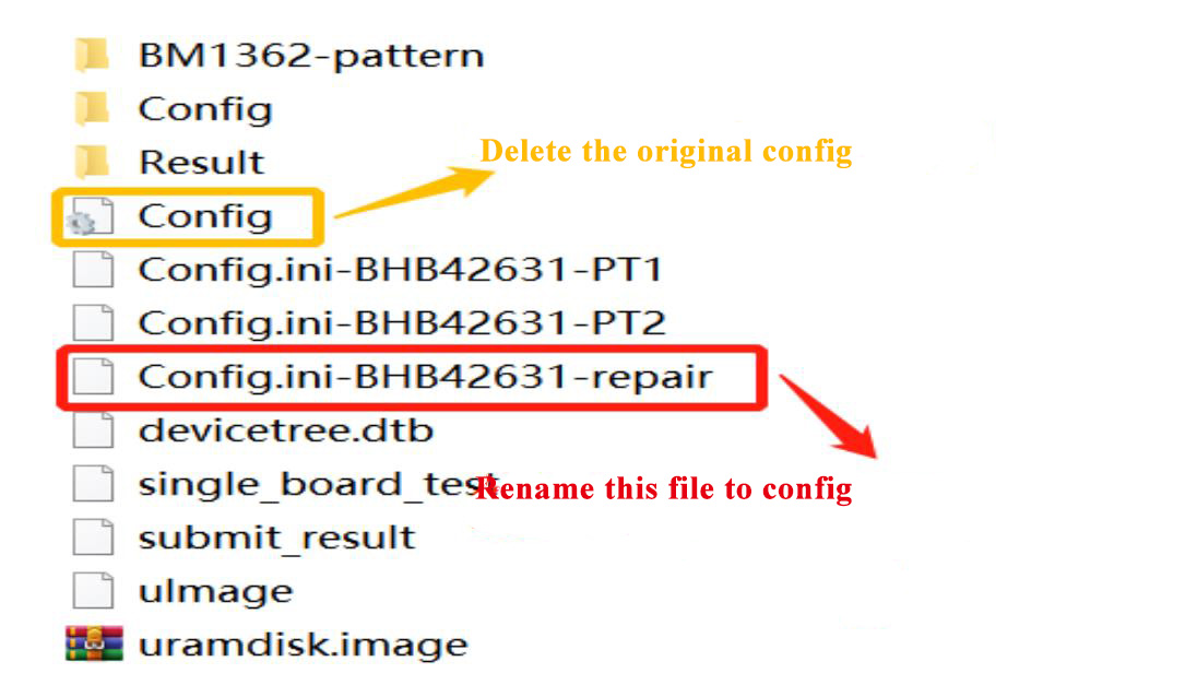
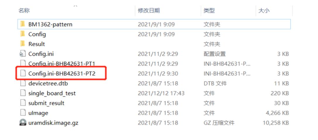
4. Setup of SD card without heatsink: The double-sided heatsink 8 x Pattern test requires the setup of SD cards, as indicated below. Change the file name "congfig ini-BHB42631-PT2" to "config ini". PT2 test can be conducted without inserting the code scanner, only inserting the network cables. For heat dissipation, please refer to the setup of heat dissipation tool (Essentials: the board is inserted into the chassis, lock screw for power supply, fans need to be at full speed with ambient temperature less than 30 °C).
IV. Principle and Structure of Hash board
1.Working structure of S19j pro hash board
The hash board consists of 126 BM1362 chips, divided into 42 domains, each comprising 3 ASIC chips. The BM1362 chips used in the S19J Pro hash board operate at 0.32V.
The 42nd, 40th, 38th and 36th groups (4 groups in total) are powered by the 20V output from the boost circuit U238 to the LD0 (U308, U305, U306 and U307), so that the LDO of these 4 domains outputs 1.2V and 0.8V. The remaining domain LDO's are powered by VDD15V input, making them output 1.2V and 0.8V.
Attention: PT2 test, we can view on the back-end log page and start counting from asic0, as shown below:
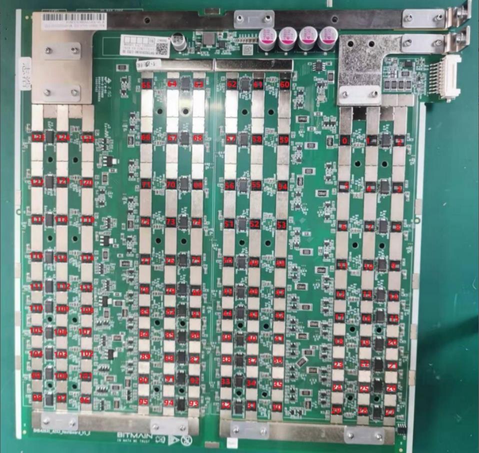
The voltage domain in the test log is counted from 0, i.e. domain0, as shown below:
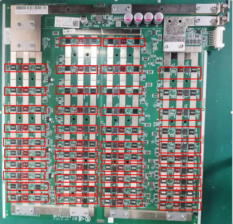
2. S19j pro hash board boost circuit, which will boost the power from 15V to 20V. As showing:


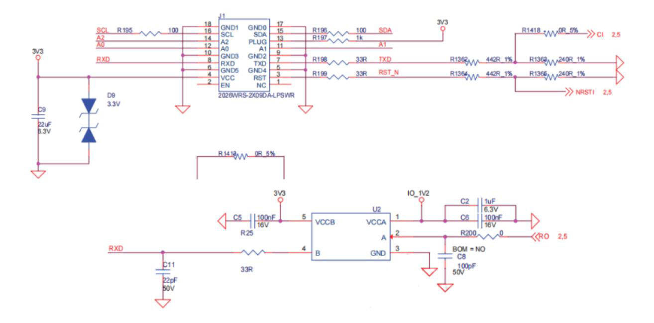
3. Signal direction of S19J PRO chip.
(1) CLK (XIN) signal flow: generated by the Y125M crystal, transmitted from chip 01 to 126; voltage is about 0.5V-0.6V
(2) RST signal flow: from the IO port pin 3, and then transmitted from chip 01 to 126.
(3) CI signal flow: from IO port pin 7, and then transmitted from chip 01 to 126.
(4) RX (RI) signal flow: from chip 126 to 01, and then return to pin 8 of IO port via U2.
(5) BO (BI) signal flow: transmitted from chip 01 to chip 126.
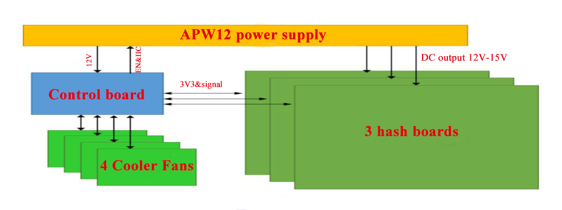
4. Architecture of the complete machine:
The machine is mainly composed of 3 hash boards, 1 control board, an APW12 1215 power supply and 4 cooling fans.
V. Common failures of hashboard and troubleshooting steps
1. Issue: single board test reports "ASIC=0"error (PT1/PT2 mode)
Step 1: troubleshoot the power output
Step 2: check the voltage output of voltage domain
Each voltage domain has the voltage of about 0.32V, and 15V power generally has domain voltage. Priority should be given to the measurement of power terminal output of hashboard.
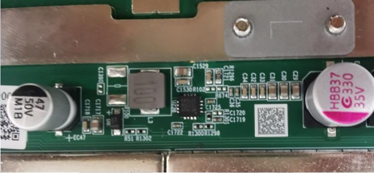
Step 3: check the output of boost circuit
In test figure, C29 capacitor can measure the voltage of 19-20V.

Step 4: Check each group of LDO1.2V or PLL0.8V output.
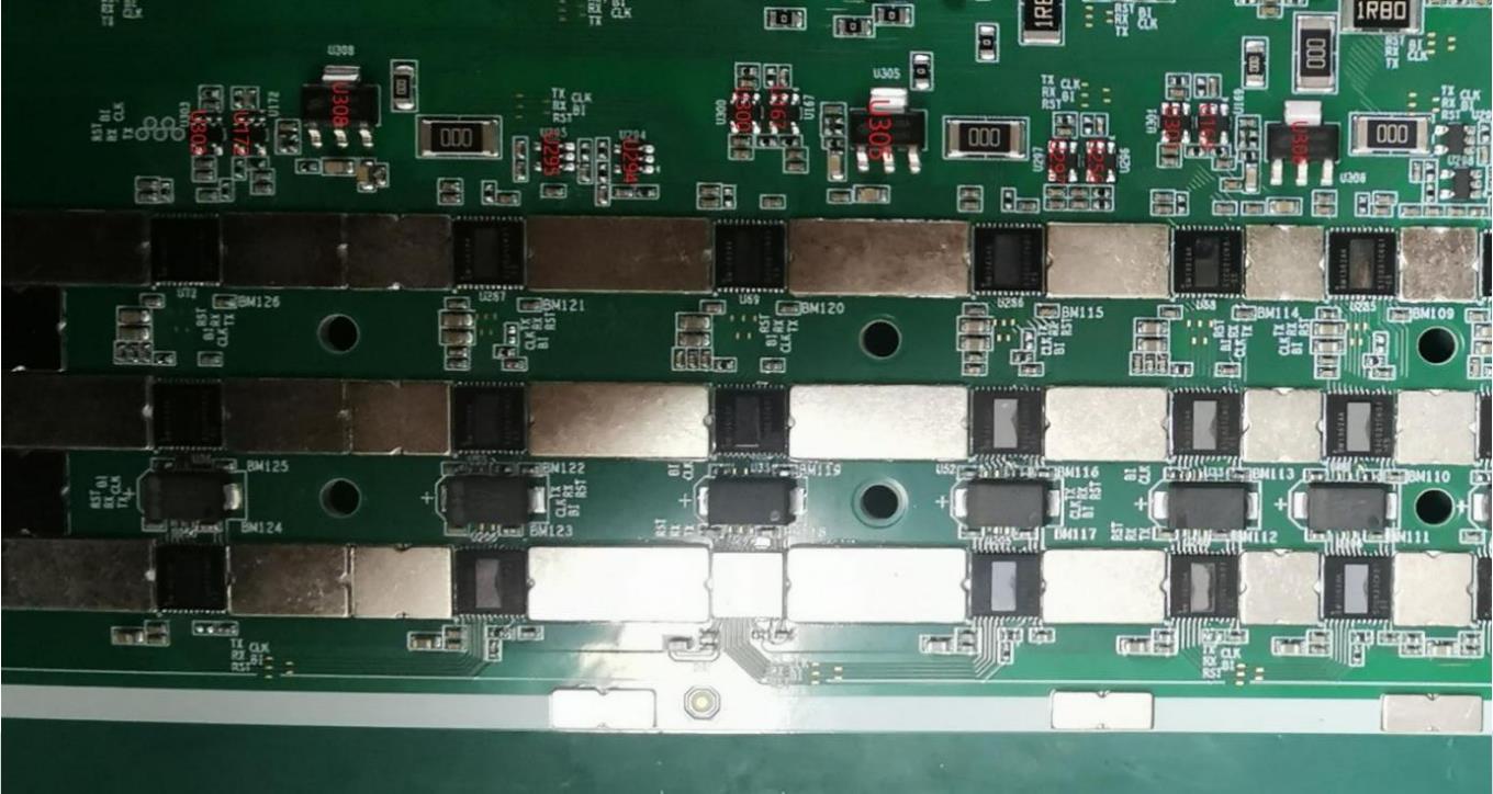
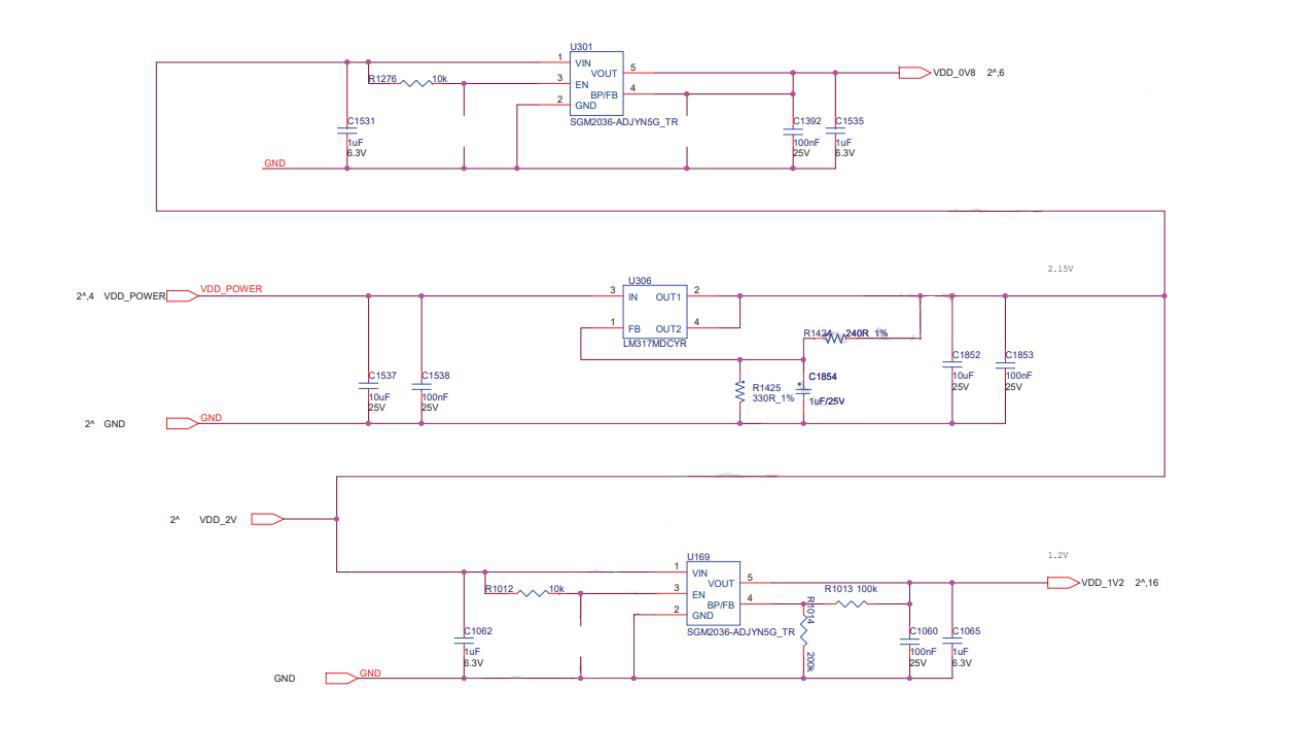
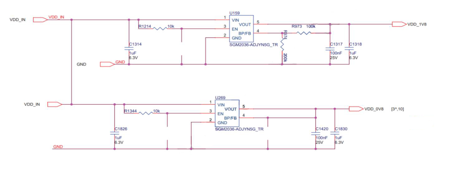
Step 5: Check the signal output of chip (CLK / CI / RI / BO / RST).
Refer to the described voltage value range based on the signal direction, and if a large deviation occurs to the voltage value during measurement, compare with the adjacent group of measured values to make a determination.
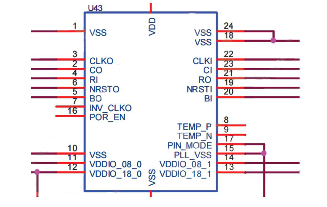
2. Issue: single board test reveals incomplete chip (PT1 / PT2 mode)
(1) When ASICNG =(0) is displayed: measure the total voltage of the domain and boost circuit 20V, and then use the shorting probe to short the RX test point and 1V2 test point in the middle of the first and second chip. Run to find the chip program, view the serial port log. If 0 chip is found, it may relate to one of the following cases:
a-1) Check whether the 1V and 0V8 test points are 1.2V and 0.8V by using a multimeter to measure the voltage. If not, it can be determined that the domain of 1.2V, 0.8V LDO circuit has abnormalities, or the two ASIC chins in the domain are not soldered, or the problem is caused by the short-circuited 0.8V and 1.2V chip filter capacitor, or the LDO circuit in the domain suffers from IC insufficient / false solder / material damage.
a-2) Detect whether the circuit of U2 is abnormal, such as insufficient soldering of resistor.
a-3) Detect if the first chip has pins that are not soldered (there are cases where the pins have tin from the side during the repair, but after removing the chip, the pins are found to be untinned).
(2) If you can find a chip in step (1), it means that the first chip and the previous circuit are good, in a similar way, check the chips behind. For example, short circuit the 1V2 and RX test points between the 23rd and 24th chip. If the log can find 23 chips, the first 23 chips are good. If you still find 0 chips, you need to first check whether the 1V2 is normal, if it is normal, the chips following 38# chip have problems.Continue to use the dichotomous method to check until we find a problematic chip. Suppose the Nth chip has a problem, then when the 1V2 and RX between the N-1th and the Nth chip are short circuited, we can find N-1 chip, but we cannot find all the chips if the 1V2 and RX between the N and the N+1 chip are short circuited.
(3) When ASIC = 125 is displayed: that is, 125 chips can be found, indicating that the hash board can detect 126 chips at 115200 baud rate, but only 125 chips are found at 12M baud rate, and one chip is not found at 12M baud rate.
Repair method: use the dichotomous method, short the probe, and short circuit 1.2V/RX.
Example: short circuit the 1V2 test points and RX test points between the 46th and 47th pin, if the log shows reading 46 chips, the first 46 chips have no problem; if the signal points between the 47th and 48th chip are short circuited, log still shows reading 46 chins, and the 47th chin cannot be detected. The appearance inspection is OK, and generally it is only required to replace the 47th chip.
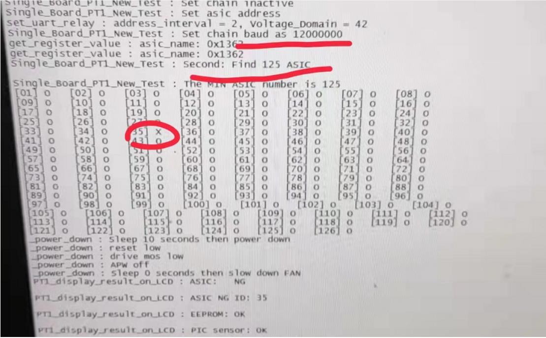
(4) When ASICNG is displayed: (constantly reporting the chip with a fixed number), there are two cases as follows:
① The first case: (usually the value of the reported chip does not change during each test), in such a situation repair can be conducted according to the normal maintenance method of measuring the signal voltage. (There may also be a resistor near the chip).
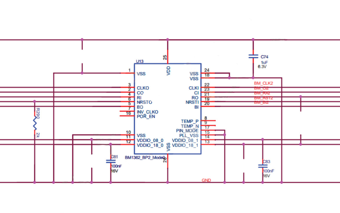
② Second case: test time is about twice as long as the good board (there will be a change in the value of X per test, sometimes X = 0);
Usually log shows the following information (where the red number is not necessarily 13, depending on which test is connected to the line):
During the test, assuming that the domain voltage of all the domains in front of the abnormal position is almost all less than 0.32V, while the domain voltage of the rear domain is almost all higher than 0.32V, this case is caused by the unsoldered chip, usually 1.2V, 0.8V, RXT and CLK are not well soldered. It is recommended to measure the domain voltage directly to locate in which domain the problem is. In section (1). 1V8 and RO short circuit is used in the same way to locate the abnormality.
3. Issue: single board test reports "Pattern NG" error, that is, nonce data is incomplete (PT2 mode).
Pattern NG is caused by the characteristics of the chip and other chips with large differences. The chips with breakage usually should only be replaced.
According to the log information, the replacement rules are as follows:
(1) Check the quality of thermal conductive gel printing.
(2) If the chip is free from damage in appearance, replace the chip with the lowest response rate in each domain.
(3) Exchange the one with higher response rate with the one with the lower response rate, see whether it follows the chip, if yes, replace the chip, if not, measure whether the domain voltage is lower than the normal value, and whether the chip pad pins have the same resistance value as normal one, if not, check whether the small resistance value is on the high side, if yes, replace it.
PS: please note that domain and asic number start from 0.
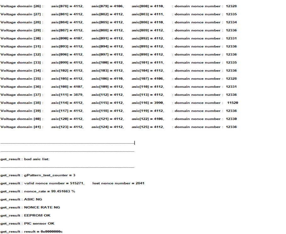
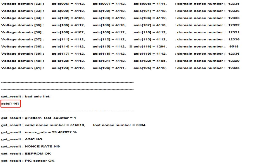
4. Issue: B_AXPCS (X chips reply insufficient)
Repair method: Swap and replace these chips with those with high response in other domains to see if they are effective. If they are ineffective, replace these chips; For example, asic116 (the 117th one) in the following figure:
5. Issue: chip test is OK, serial port does not stop (long-time operation) during PT2 function test
Repair method: In PT2 test, look at the serial port print log, if the serial port begins to run for a long time, use the short-circuit probe to short-circuit RX & 1.2V from the first chip. If the serial port stops running for a long time after the short circuit, it means that the first chip is OK. Use this method to find the chip that still has a long run fault after a short circuit. It is usually caused by a broken chip. Replace it;
Requirements for PT2 test environment: PT2 test environment should be at 20 to 30 degrees. When the ambient temperature exceeds 35 degrees, the software will stop testing. Heat dissipation is required for measurement. The following heat dissipation platforms can be used for PT1 measurement and run DEBUG firmware.
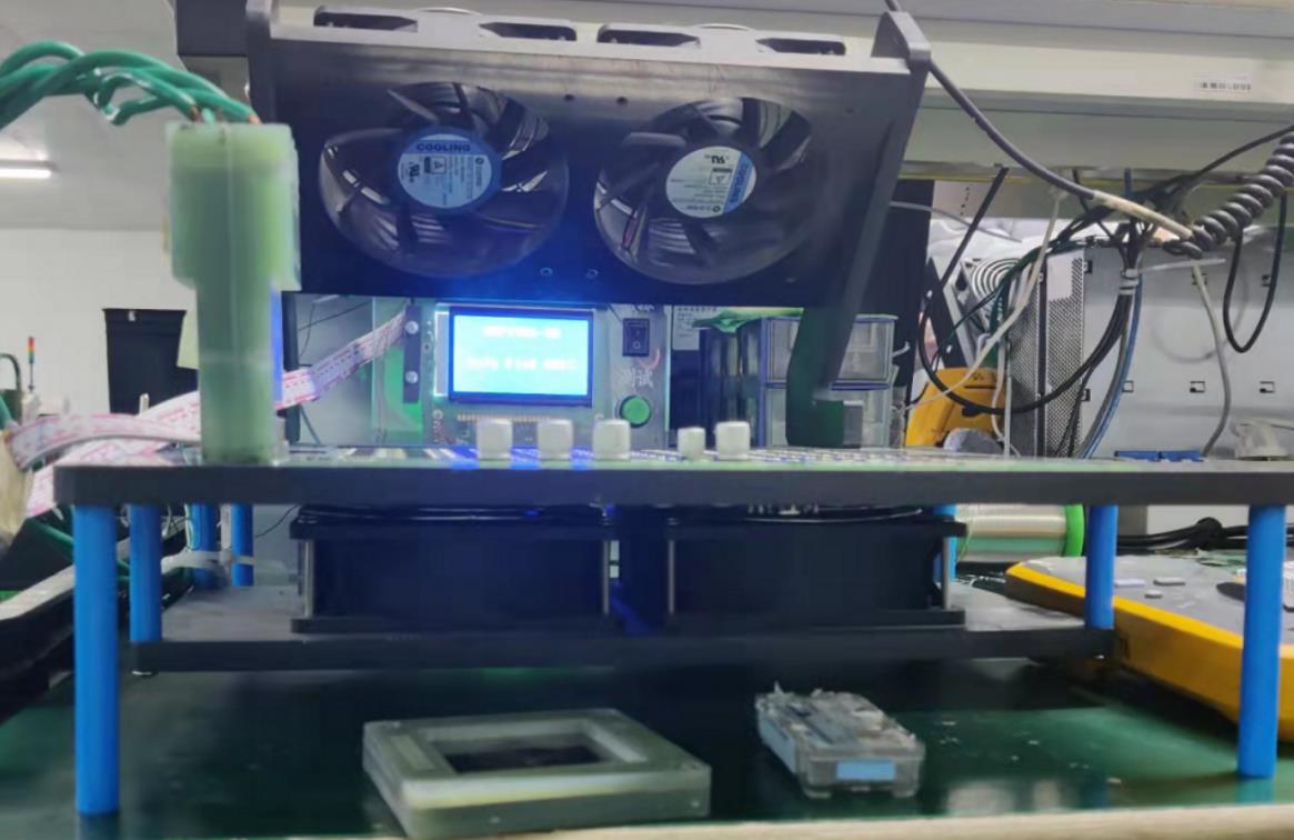
Power supply requirements for PT2 test: under a 1500-watt load (test a board), the actual voltage output by PT2 test fixture cannot be lower than the 0.03V set by the configuration file. (For example, the configuration file requires a trial run of 15V, then when the power supply is loaded with 1500 watts. the output voltage cannot be lower than 14.97V).
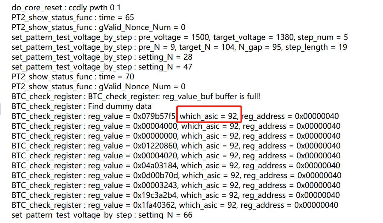
6. Chip address error (PT2)
Repair method: replace the chip with error reporting.
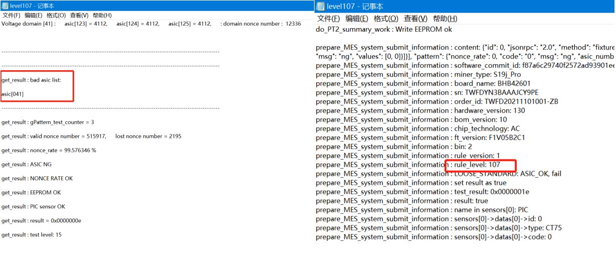
7. LEVEL100+: individual chips cannot meet the test criteria
Repair method: repair according to the log RESULT.
Ⅵ. Common Issue of the Control Board and Troubleshooting Steps
1. The whole machine does not run
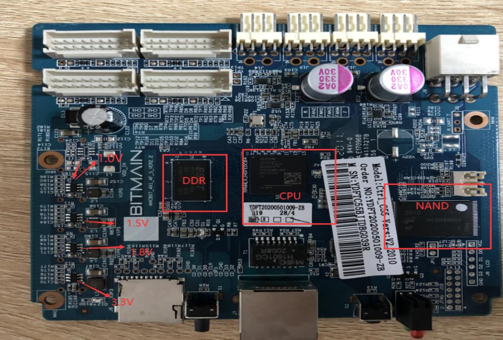
(1) Check whether the voltage of several voltage output points are normal. In case of 3.3V short circuit, first disconnect U8, and if short circuit still exists, unplug CPU and then measure again. Other voltage abnormalities generally replace the corresponding voltage IC.
(2) The voltage is normal, please check the welding condition of DDR / CPU.
(3) Try to update the flash program with SD card.
If the machine needs to start normally, the following two steps are required.
a) After the card swiping is successful, the green LED indicator is always on, and power off and restart.
b) Wait for 30s after re-powering (time of opening OTP).
c) OTP (OneTimeProgramable) is a memory type of MCU, which means one-time programmable. The program will not be changed and cleared
again after burning IC.
Cautions:
-Sudden power failure or the time less than 30s during the process of opening 0TP will cause the control board fail to enable OTP function and the control board wil not start (not networked). It is required to replace U1 (main control ICFBGA of control board). The replaced U1 cannot be used in ANTMINER 19 series miners.
-For the control board that has enabled the OTP function, U1 cannot be used on other model series.
2. The whole machine cannot find the IP.
It is highly possible that the abnormal operation results in such failure to find the IP, and refer to point 1 to troubleshoot
Check the appearance of the network port, network transformer T1 and CPU, and the welding condition.
3. The whole machine cannot be upgraded.
Check the appearance of the network port, network transformer T1 and CPU, and the welding condition
4. The whole machine fails to read the hashboard or has less chains.
A. Check the wiring connection of lines.
B. Check the parts of the control board corresponding to chains.
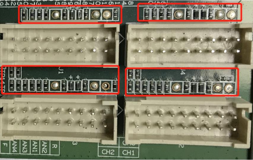
C. Check the wave soldering quality of the pins and the resistance around the plug-in interface.
VII. The Machine-level Failure
1. Initial test of the whole machine.
Abnormal fan display: it is necessary to check whether the fan works normally, whether the connection with the control board is normal, and whether the control board has abnormalities.
2. Less chain: three hashboards are in total, but a hashboard is missing, which is mostly caused by the link failure between the hashboard and the control board. Check whether there is an open circuit in the line, if the connection is 0K, the single board can be used for PT2 test to check whether it can pass the test. If yes, the failure possibly will lock the control board, if not, repair it using the method of repairing PT2
3. Temperature abnormalities: The maximum PCB temperature set by our monitoring system cannot exceed 90℃ / 194°F. If it exceeds 90℃, the machine will alarm and cannot work normally. Generally, it is caused by too high ambient temperature. In addition, abnormal fan operation will also cause abnormal temperature.
4. Fail to find all the chips: (The machine can operate. but the hash is 2/3 or 1/3 of the normal value) The number of chips is not enough. Please refer to PT2 for testing and maintenance.
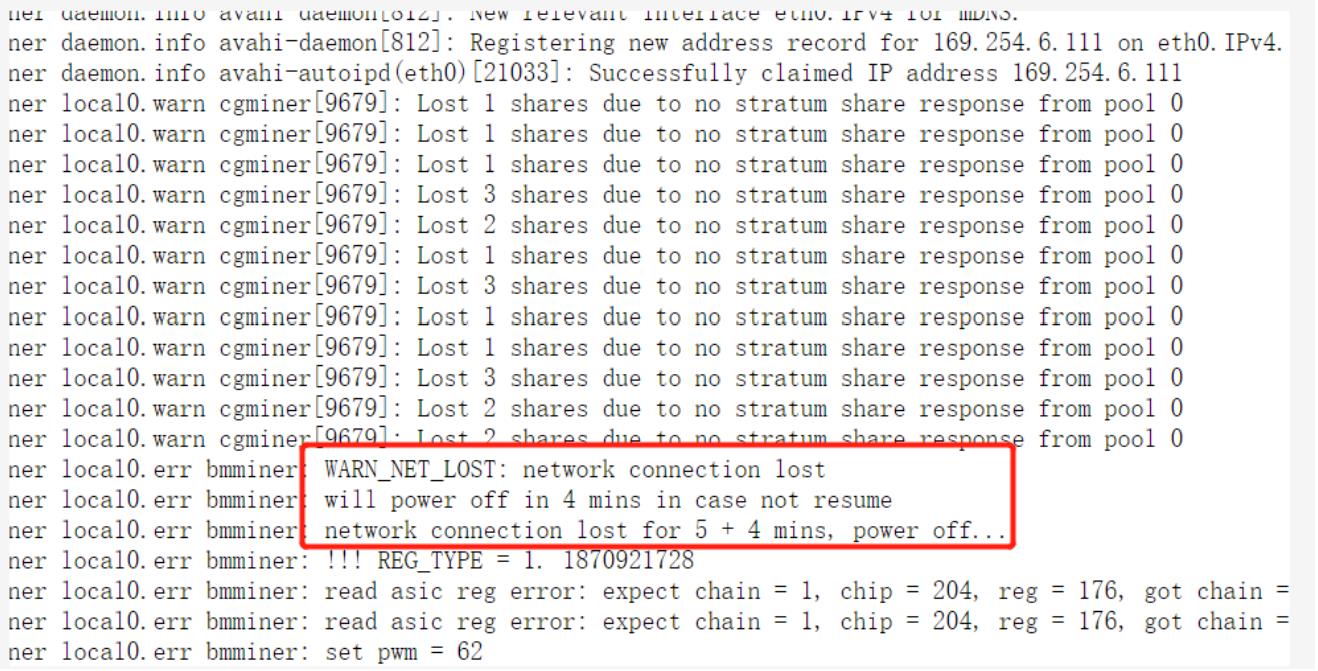
5. No hash after running for a period of time, the mining pool connection is interrupted, and it is required to check the network.
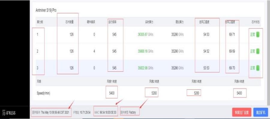
6. After the board is tested OK and assembled into a complete machine.
Low hash occurs: as shown in the figure below, the first plate has no hash after running for about 3 minutes.
Specific analysis methods are as follows: First, perform a board PT2 test to see if the board has normal performance. If the test chip is not complete, the board needs to be repaired. If it is normal after the test, take out the board separately, use the test fixture to transport the master board program of Debug for mining, and adjust the fan wind speed to 95%. The voltage and frequency are adjusted to the working voltage and frequency of the whole machine, so that the machine can mine and check whether there is any hash loss. If any, reduce the frequency to 200M, and other conditions remain unchanged. Let the machine to mine to see if there is a hash loss and if the hash board can perform X. If X and hash rate drop still occur, remove the heat sink from the hash board to mine. In the event of hash loss, measure the domain voltage to see if it is normal, in general, the domain voltage will be abnormal in problematic domains. Measure the Rl signal to see where the RI signal is interrupted. If the RI signal disappears, we can basically determine that the chip is short-circuited or damaged after continuous tin electrode posit.
Ⅷ. Other Precautions
Flow Chart of Maintenance:

1. Routine inspection:
(1) First, visually inspect the hashboard to see if there is PCB deformation or burning. If any, it must be handled first.
(2) Visually inspect whether there are obvious burning marks on parts, parts impact offset or missing parts.
(3) After visual inspection, the impedance of each voltage domain can be detected to check for short circuit or open circuit. If any, it must be handled first.
(4) Check whether the voltage of each domain is about 0.32V.
2. After the routine detection is OK (for the general routine detection, short circuit detection is necessary to avoid burning the chip or other materials due to short circuit when the power is on), the test fixture can be used for chip detection, and the judgment and locating can be
made according to the test fixture detection results.
3. According to the display results of test fixture, start from the vicinity of the faulty chip to detect the voltage at the chip test point (CO / NRST / RX / XIN / BI) and VDDOV8, VDD1V2, etc.
4. According to the signal flow direction, except RX signal, it is transmitted in reverse (chip 126 to chip 1). Several signals CLK / CO / BO / RT are transmitted in forward direction (1-126), and abnormal fault points are found through power supply sequence.
5. When locating the faulty chip, it is necessary to reweld the chip. The method is to add flux around the chip (preferably no cleaning flux), heat each solder joint of the chip pin to the dissolved state, and make the chip pin and pad run in and accept tin, so as to achieve the effect of re-tinning. If the same fault still exists after re-soldering, the chip can be replaced directly.
6. The repaired hashboard must pass the test more than twice before it can be judged as a good product. For the first time, after the parts are replaced, wait for the hashboard to cool down, use the test fixture to test, and then put it aside to cool down. For the second time, wait for the hashboard to cool down completely before testing.
Dear Customers,
Hello, May 1-5, 2026 (GMT+8) is China's May Day, and international logistics will be suspended. Our company will suspend shipments on the afternoon of April 30, 2026, and resume warehouse shipments on May 6 (GMT+8). We are deeply sorry for the inconvenience caused to you. Thank you for your trust and support.
Best wishes,
ZEUS MINING CO., LTD.