

The article details the repair methods, electrical architecture, and hardware rework process for the M54 and M64 series hydro-cooling miner.
1. Diagnostic Workstation Configuration and Essential Equipment
1.1 Test Software
Using the Moxterm software for testing. Should this utility be unavailable on the service workstation, request a copy from the technical support team before proceeding.
1.2 Test Commands
The following describes the test commands:
Hashboard test | ft-readchipid |
First 9 groups LDO power on | echo 1 > /sys/class/gpio/gpio263/value |
Test cable connect to slot0, 1 | |
RST set to 1.2V | echo 1 > /sys/class/gpio/gpio201/value |
RST set to 0V | echo 0 > /sys/class/gpio/gpio201/value |
Test cable connect to slot2, 3 | |
RST set to 1.2V | echo 1 > /sys/class/gpio/gpio202/value |
RST set to 0V | echo 0 > /sys/class/gpio/gpio202/value |
1.3 Diagnostic Control Board
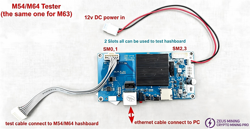
The test fixture employs a standard hydro-cooler control board (compatible with CB4/CB5/CB6 variants). Critical Note: While this jig board and its associated test firmware are interchangeable with the M63 series, the factory-fitted control boards supplied with M54/M64 units are write-protected and cannot be re-flashed; they are therefore unsuitable for use as diagnostic fixtures.
1.4 Test cable
The test cable is the original cable for the hydro-cooling miner.
1.5 Test fixture control board connection
Connect as shown in the diagram below.
1.6 Power Delivery Specifications
· Hashboard Power Supply Calculation Rule:
The operating voltage is a function of the total series stages. The base calculation is 0.31 V * (Total number of voltage domains). Each domain comprises three consecutive ASIC chips.
Example: If Slot 0 and Slot 1 each host 96 chips, the combined count is 192 chips. Dividing by 3 yields 64 domains. The resultant test voltage is 0.31*64 = 19.84V, which may be rounded to a practical setting of 20 VDC.
· Control Board Logic Supply:
A stable 12 VDC and 2A input is mandatory for the fixture control board.
1.7 Required Rework and Measurement Toolkit
Soldering Platform: Hot-air rework station.
Instrumentation: Digital multimeter and oscilloscope.
Consumables and Hand Tools: Fine-tip tweezers, solder paste, and activated rosin flux.
2. Circuit Structure Introduction
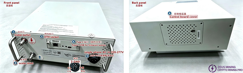
2.1 External Panel Layout
The interface of the chassis integrates six functional modules:
(1) Water outlet
(2) Water outlet
(3) Ethernet socket for network connetion
(4) USB Type-C receptacle for firmware flashing
(5) Power input terminal
(6) A control board cover.
2.2 ASIC Chip Series - Connected power supply
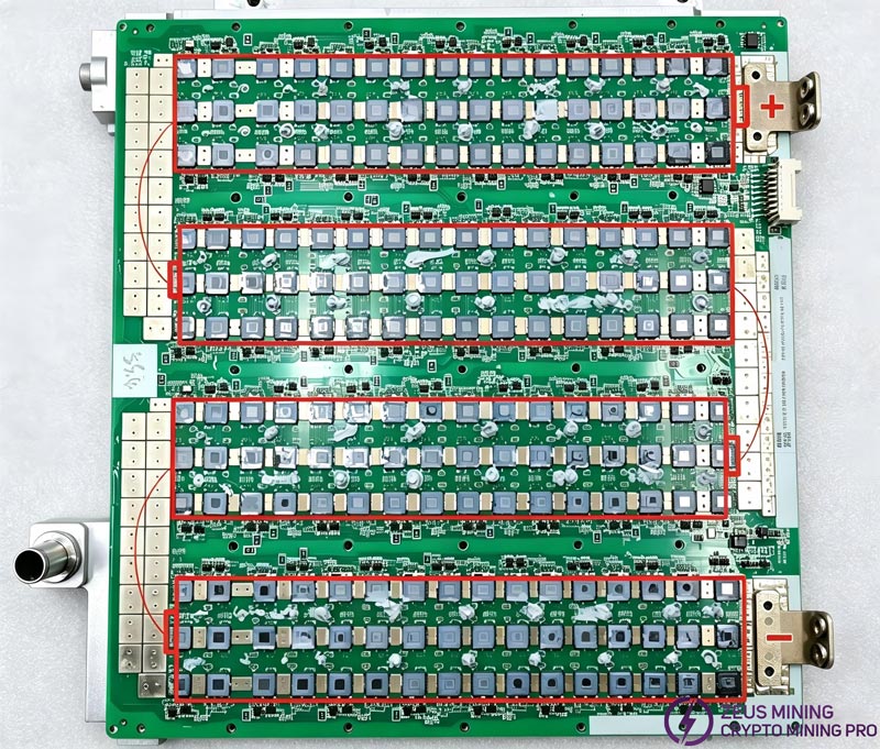
The diagram below shows four rows of chips on a hash board connected in series (from top to bottom):
· The copper power rail in the upper left corner is the positive terminal.
· The copper power rail in the lower right corner is the negative terminal.
Note: The connection between the positive and negative terminals constitutes the power supply circuit of the chipset.
2.3 LDO Power Supply Stratification
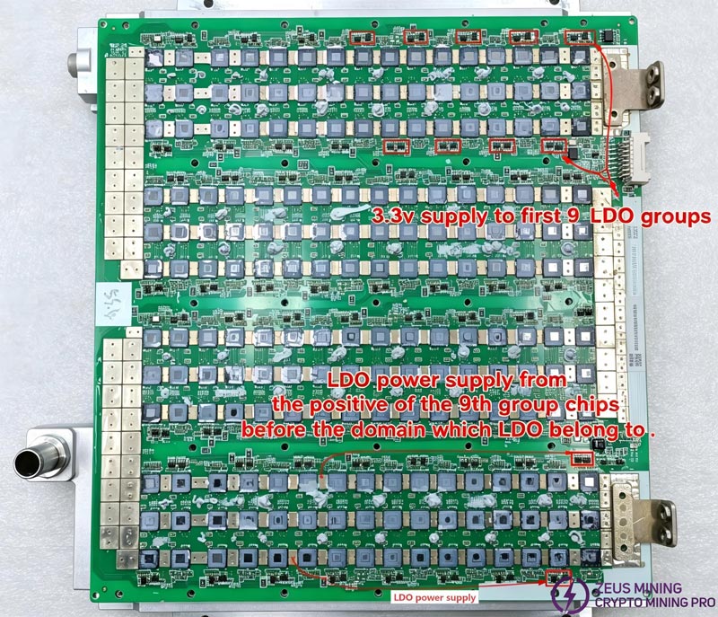
The power input of the first 9 LDOs is provided by the control board. These LDOs remain inactive in the initial (pre-power-on) state. After executing the power-on command "echo 1 > /sys/class/gpio/gpio263/value", the control board supplies 3.3 V voltage to the first 9 LDOs.
The input voltage of other LDOs comes from the positive pole of the ninth group chip, and is fed into the first pin of the LDO via a 4R7 resistor.
2.4 Signals of ASIC chips
The hashboard’s logic domain is partitioned into two primary blocks, labeled SM0 and SM1. Four core signals (RST, CLK, RXD, TXD) are transmitted on the hash board.
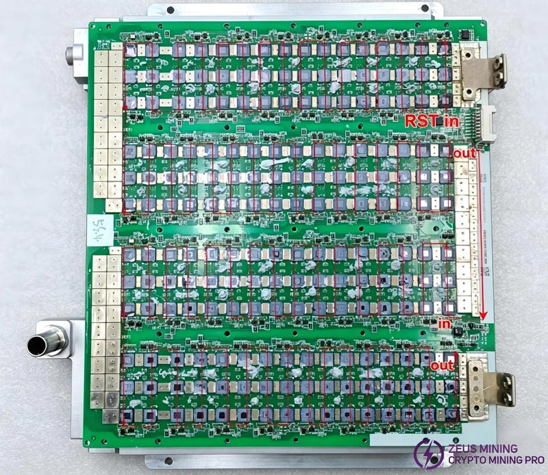
RST signal: This is a public signal. It enters from the first chip of SM0, passes through all the chips in SM0 in sequence, and then exits from SM0 and enters the first chip of SM1. After exiting from the last chip of SM1, it drives an LED to indicate the high/low level state of the RST signal.
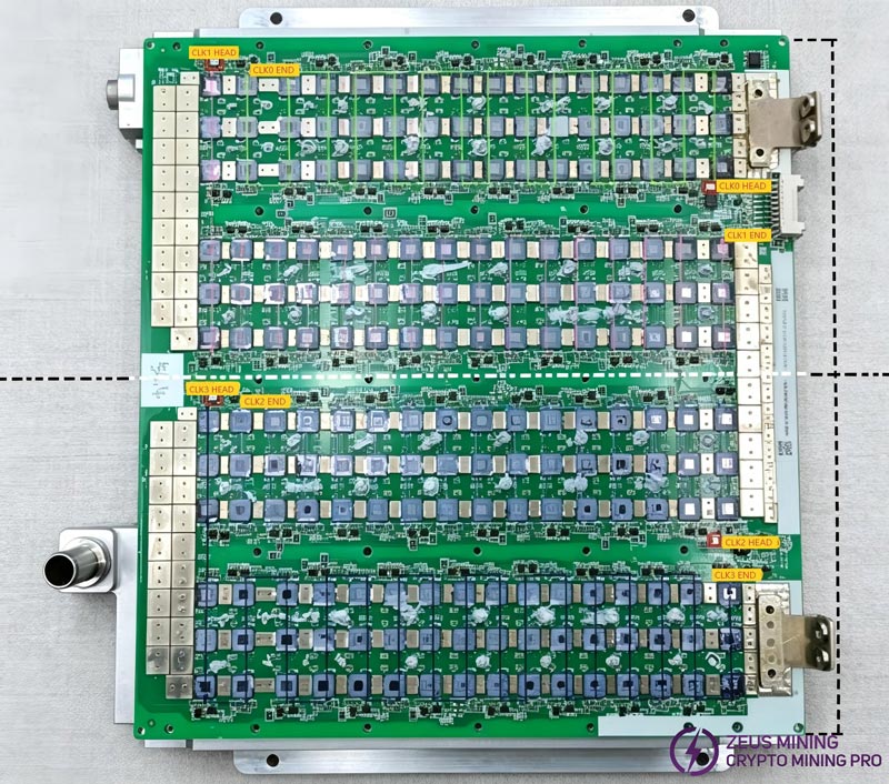
CLK signal: It is generated by a crystal oscillator (each oscillator is responsible for signal transmission over a specific distance). As shown in the figure, the clock signal needs to be checked in segments.
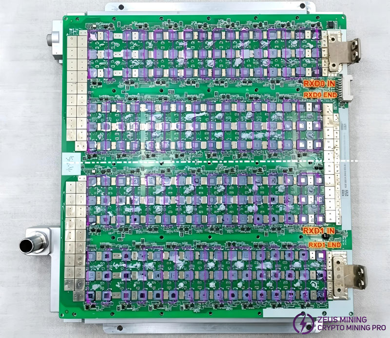
RXD signal: Upper segment: Input from the first chip, terminated at the last chip. Lower segment: Input from the first chip, terminated at the last chip. The upper and lower segments operate independently.
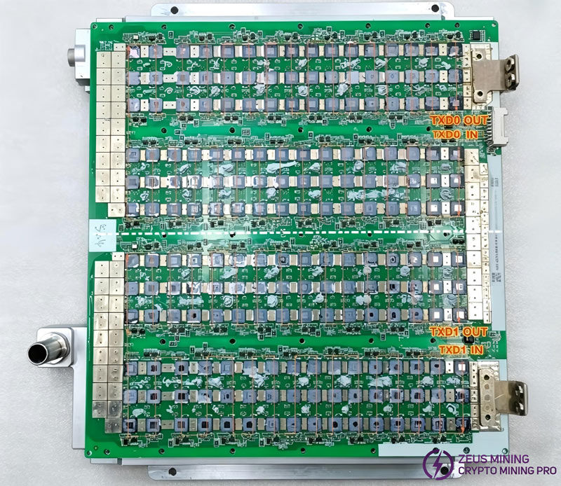
TXD Signal: Upper Segment: Enters from the last chip and returns to the first chip. Lower Segment: Enters from the last chip and returns to the first chip. The upper and lower segments operate independently.
2.5 SM0 Slot Signal Routing Schematic
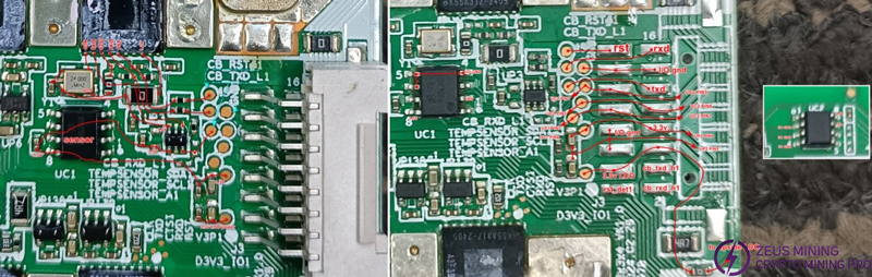
The following two diagrams show the physical signal routing layout of the SM0 I/O port (left), i.e., the detailed signal routing diagram of the SM0 I/O port. The right diagram shows the signal connections of each pin of the SM0 I/O port, i.e., pin-level signal connection diagram of the SM0 I/O port).
2.6 SM1 Port Signal Routing Diagram
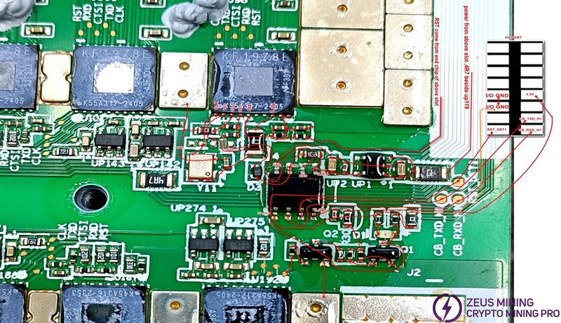
In the diagram below, UP1 outputs 2.5V to power the bidirectional level shifter chip UP2. Simultaneously, UP2 converts the RXD and TXD signals of slot 1.
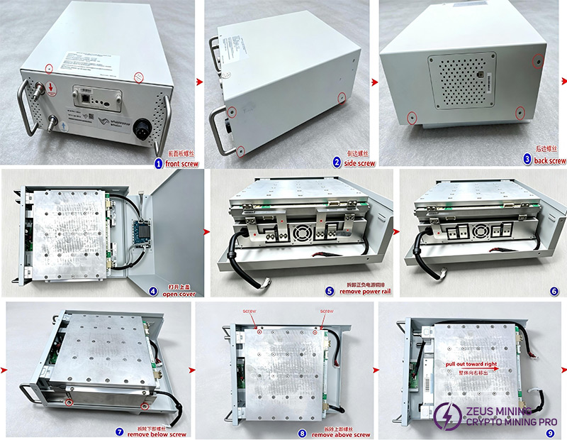
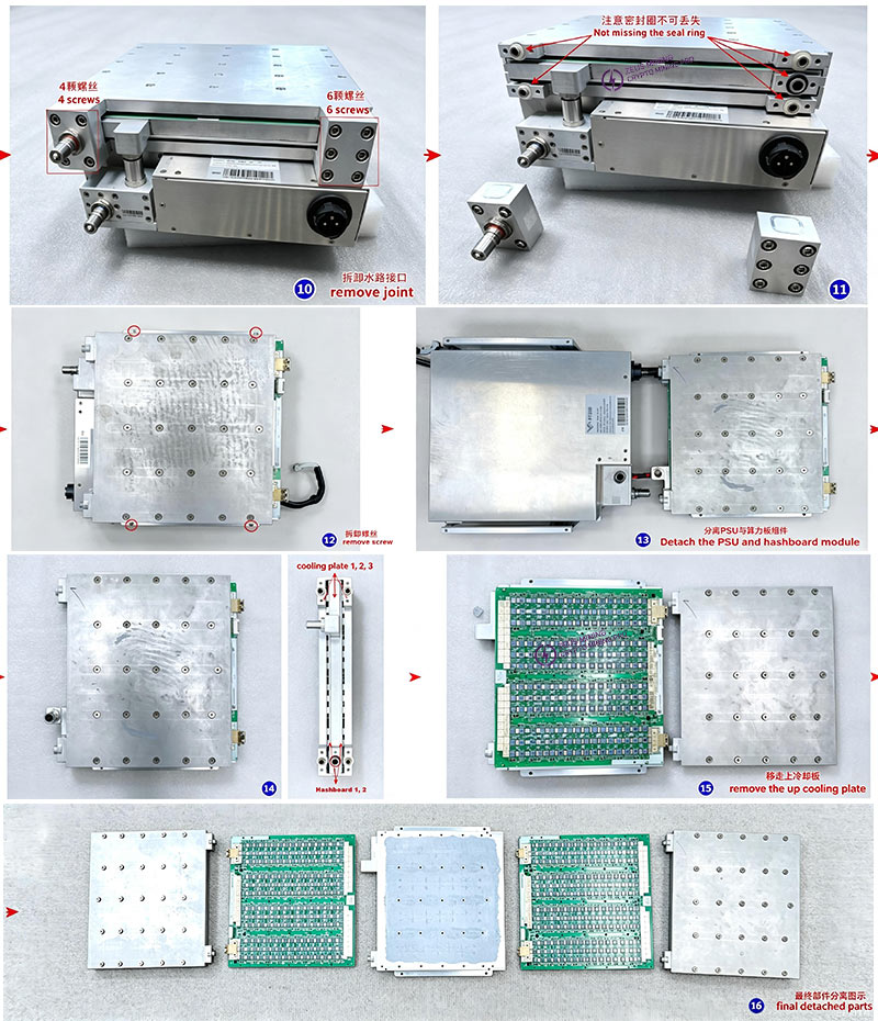
3. M54 and M64 Series Removal and Installation Procedures
• Removal: Perform steps 1 through 16 in sequence.
• Assembly: Begin with step 16 and proceed downwards until step 1.
4. Hashboard Installation Location
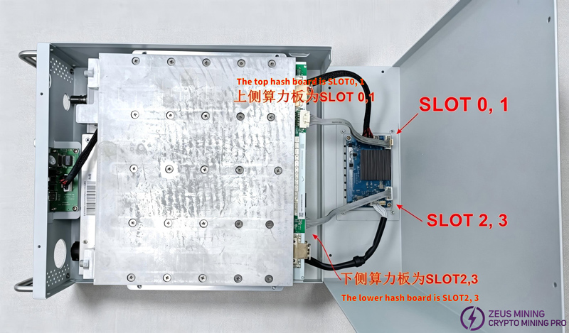
After opening the top cover of the hydro-cooling miner (M54 & M64 series), the slots in the upper area correspond to slots 0 and 1, and the slots in the lower area correspond to slots 2 and 3. Please refer to the diagram below for details.
5. Basic Repair Procedures
Step 1: Check if the output voltage of each LDO is normal.
Step 2: Check the RST signal of the entire hash board to ensure it is functioning correctly.
Step 3: Check the CLK signal segment by segment to ensure its frequency is stable at 24 MHz.
Step 4: Check the RXD signals of the upper and lower sections separately.
Step 5: Check the TXD signals of the upper and lower sections separately.
6. Maintenance Case
If error code 560 (Fault Description: Balance Loss) appears during the operation of a hydro-cooling miner, please follow the steps below for troubleshooting.
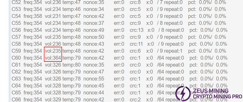
In the diagram above, VOL represents the chip's operating voltage. The VOL value changes abruptly starting from C60. For hydro-cooling miners that have been removed from the cabinet, you can use a multimeter to measure the LDO output pin PIN5 of the chipset containing the U61 hash board. You may find the voltage is too low, usually due to a faulty chip in the chipset causing the LDO output voltage to drop. In this case, you can identify and replace the faulty chip.
7. Precautions
• Before disassembling the water-cooled miner (M54 & M64 series), the liquid inside the cooling plates must be completely drained using an air pump.
• After the water-cooled miner has been repaired and passed performance testing, the liquid inside the cooling plates must be completely drained again using an air pump.
 China Mainland Hong Kong
 Business Hours: (GMT+8) 08:30-20:00 Mon to Sat
 Company Phone: +86-023-72227777