

BM1384 is a kind of high-performance and low-power consumption bitcoin mining ASIC for Antminer S5.
1. Feature
• Typical hash rate and power
Voltage(V) | Hash Rate(GH/S) | Current(A) | Total power(W) | W/GH |
0.80 | 22.00 | 12.310 | 9.848 | 0.448 |
0.75 | 17.88 | 9.200 | 6.900 | 0.386 |
0.72 | 15.13 | 7.440 | 5.357 | 0.354 |
0.70 | 13.75 | 6.600 | 4.620 | 0.336 |
0.65 | 11.00 | 4.460 | 2.899 | 0.264 |
0.60 | 8.25 | 3.430 | 2.058 | 0.249 |
• Customized package
• Support UART communication interface
• Support chain mode, Max 256 chips per chain
• Support hardware addressing and software addressing
2. Applications
Bitcoin mining for Antminer S5
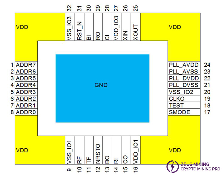
1. Pin diagram

2. Signal Description
Name | I/O | Active Level | Description |
XIN | I | N/A | Oscillator input |
XOUT | O | N/A | Oscillator output |
RST_N | I | L | Reset signal |
TEST | I | N/A | Internal pull down. 0: Normal mode 1: Test mode |
SMODE | I | N/A | Serial Mode. Internal pull up. 0: Asynchronous UART mode. 1: Synchronous UART mode. |
CLKOUT | O | N/A | Clock output |
NRSTO | O | L | Reset output |
CI | I | N/A | Command Input. Schmitt input. |
CO | O | N/A | Command Output |
RI | I | N/A | Respond Input. Schmitt input and internal pullup. |
RO | O | N/A | Respond Output |
BI | I | H | Respond Busy Input. Schmit input and internal pulldown. |
BO | O | H | Respond Busy Output |
ADDR[7:0] | Address Input. Internal pullup. | ||
RF | O | RO open drain output; Command Rx Flag | |
TF | O | Respond Tx Flag | |
PLL_VDD | PLL analog power (1.8V) | ||
PLL_VSS | PLL analog ground | ||
LDO_DVDD | PLL analog power (0.9V) | ||
LDO_DVSS | PLL digital ground |
Clock Freq. (M) | Hash rate (G) | Reg. value | Ideal delay (ms) | Recommend delay (ms) |
100 | 5.500 | 0783 | 12.2 | 11 |
125 | 6.875 | 0983 | 9.8 | 9 |
150 | 8.250 | 0b83 | 8.1 | 7 |
175 | 9.625 | 0d83 | 7.0 | 6 |
200 | 11.000 | 0782 | 6.1 | 5 |
225 | 12.375 | 0882 | 5.4 | 5 |
250 | 13.750 | 0982 | 4.9 | 4 |
275 | 15.125 | 0a82 | 4.4 | 4 |
300 | 16.500 | 0b82 | 4.1 | 4 |
325 | 17.875 | 0c82 | 3.8 | 3 |
350 | 19.250 | 0d82 | 3.5 | 3 |
375 | 20.625 | 0e82 | 3.3 | 3 |
400 | 22.000 | 08f2 | 3.0 | 3 |
425 | 23.375 | 0801 | 2.9 | 3 |
450 | 24.750 | 0881 | 2.7 | 2 |
Programming the Output Clock Frequency
FREF=FIN/NR
FVCO=FOUT*NO
FOUT=FIN*NF/(NR*NO). where FREF is the comparison frequency for the PFD. For proper operation in normal mode, the following constraints must be satisfied
Input Divider Value(NR)
NR =16*R[4] + 8*R[3] + 4*R[2] + 2*R[1] +R[0] +1 =R[4:0] + 1
Feedback Divider Value (NF)
NF =2*(64*F[6]+32*F[5]+16*F[4]+8*F[3] +4*F[2] +2*F[1]+F[0] +1) = 2*(F[6:0]+1)
Output Divider Value(NO)
OD[1:0] | 002 | 012 | 102 | 112 |
NO | 1 | 2 | 4 | 8 |
Table. 4 PLL output divider setting table
High-band
25 MHz ≤ FREF ≤ 50 MHz
1500 MHz ≤FVCO≤3000 MHz
187.5 MHz≤FOUT≤3000 MHz
Low-Band
10 MHz≤FREE≤50 MHz
800 MHz≤FVCO≤1600 MHz
100 MHz≤FOUT≤1600 MHz
1. Absolute maximum rating
Symbol | Parameter | Max value | Unit |
VDD | Core Voltage | 1.2 | V |
VCC | IO Voltage | 1.98 | V |
PLL_DVDD | PLL Digital power | 1.2 | V |
PLL_AVDD | PLL analog Power | 1.92 | V |
TSTG | Storage Temperature | -65~150 | ℃ |
2. Recommended operation conditions
Symbol | Parameter | Min. | Typ. | Max. | Unit |
VDD | Core Voltage | 0.65 | 0.8 | 1.1 | V |
IO_VDD | IO Voltage | 1.62 | 1.8 | 1.98 | V |
PLL_VDD | PLL Digital power | 0.81 | 0.9 | 0.99 | V |
PLL_AVDD | PLL analog Power | 1.62 | 1.8 | 1.98 | V |
TOPT | Operation Temperature | 0 | 25 | 125 | ℃ |
3. DC characters
Symbol | Parameter | Min. | Typ. | Max. | Unit |
VIL | Input Low Voltage | -0.3 | 0.63 | V | |
VIH | Input High Voltage | 1.17 | 1.98 | V | |
VOL | Output Low Voltage | 0.45 | V | ||
VOH | Output High Voltage | 1.35 | V | ||
IL | Input Leakage Current | ±10 | uA | ||
VT | I/O threshold point | 0.81 | 0.89 | 0.97 | V |
VT+ | Schmitt input low to high threshold pint | 0.95 | 1.03 | 1.10 | V |
VT- | Schmitt input high to low threshold pint | 0.64 | 0.75 | 0.86 | V |
RPU | I/O internal pull-up resistor | 47K | 69K | 106K | Ω |
RPD | I/O internal pull-down resistor | 49K | 85K | 159K | Ω |
ICC(VCC) | Supply current of VCC | 10 | mA | ||
ICC(PLL) | Supply current of PLL_DVDD and PLL_AVDD | 4 | mA | ||
CBIN | Input pin capacitance | 10 | pF | ||
CBOUT | Output pin capacitance | 10 | pF |

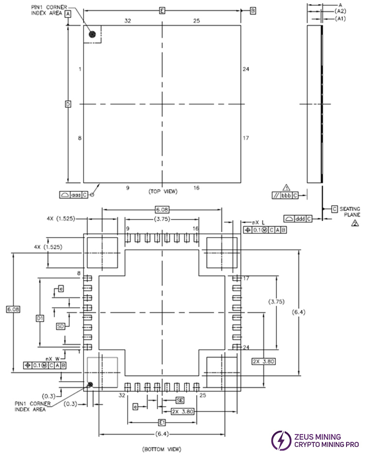
SYMBOL | COMMON DIMENSIONS | |||
MIN. | NOR. | MAX. | ||
TOTAL THICKNESS | A | 0.85 | ||
SUBSTRATE THICKNESS | A1 | 0.1 | REF | |
MOLD THICKNESS | A2 | 0.7 | REF | |
BODY SIZE | D | 8 | BSC | |
E | 8 | BSC | ||
LEAD WIDTH | W | 0.2 | 0.25 | 0.3 |
LEAD LENGTH | L | 0.35 | 0.4 | 0.45 |
LEAD PITCH | e | 0.5 | BSC | |
LEAD COUNT | n | 32 | ||
EDGE BALL CENTER TO CENTER | D1 | 3.5 | BSC | |
E1 | 3.5 | BSC | ||
BODY CENTER TO CONTACT BALL | SD | 0.25 | BSC | |
SE | 0.25 | BSC | ||
BALL WIDTH | b | |||
BALL DIAMETER | ||||
BALL OPENING | ||||
BALL PICTH | e1 | |||
BALL COUNT | n1 | |||
PRE-SOLDER | ||||
PACKAGE EDGE TOLERANCE | aaa | 0.1 | ||
MOLD FLATNESS | bbb | 0.2 | ||
COPLANARITY | ddd | 0.08 | ||
BALL OFFSET(PACKAGE) | eee | |||
BALL OFFSET(BALL) | fff | |||
Dear Customers,
Hello, May 1-5, 2026 (GMT+8) is China's May Day, and international logistics will be suspended. Our company will suspend shipments on the afternoon of May 1, 2026, and resume warehouse shipments on May 6 (GMT+8). We are deeply sorry for the inconvenience caused to you. Thank you for your trust and support.
Best wishes,
ZEUS MINING CO., LTD.